• Acta Physica Sinica
  • Vol. 69, Issue 8, 086101-1 (2020)
Chao Lu1、2, Wei Chen2、*, Yin-Hong Luo2, Li-Li Ding2, Xun Wang2, Wen Zhao2, Xiao-Qiang Guo2, and Sai Li3
Author Affiliations
  • 1Key Laboratory of Particle and Radiation Imaging of Ministry of Education, Department of Engineering Physics, Tsinghua University, Beijing 100084, China
  • 2State Key Laboratory of Intense Pulsed Radiation Simulation and Effect, Northwest Institute of Nuclear Technology, Xi’an 710024, China
  • 3National Space Science Center, Chinese Academy of Sciences, Beijing 101400, China
  • show less
    DOI: 10.7498/aps.69.20191896 Cite this Article
    Chao Lu, Wei Chen, Yin-Hong Luo, Li-Li Ding, Xun Wang, Wen Zhao, Xiao-Qiang Guo, Sai Li. Effect of source-drain conduction in single-event transient on nanoscaled bulk fin field effect transistor[J]. Acta Physica Sinica, 2020, 69(8): 086101-1 Copy Citation Text show less
    The structure of two fin FinFET device.
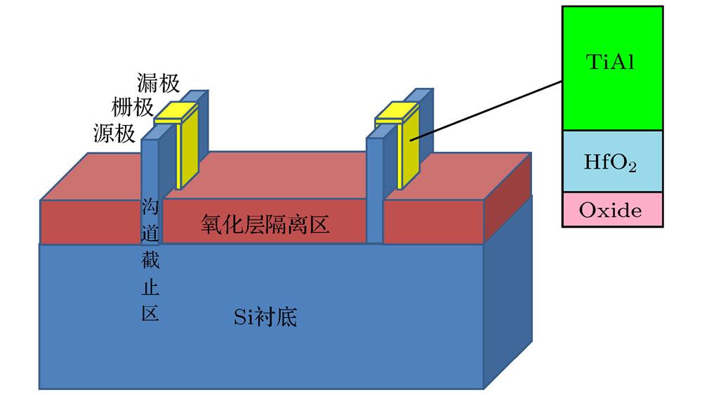
    Fig. 1. The structure of two fin FinFET device.
    The circuit schematic of experience.
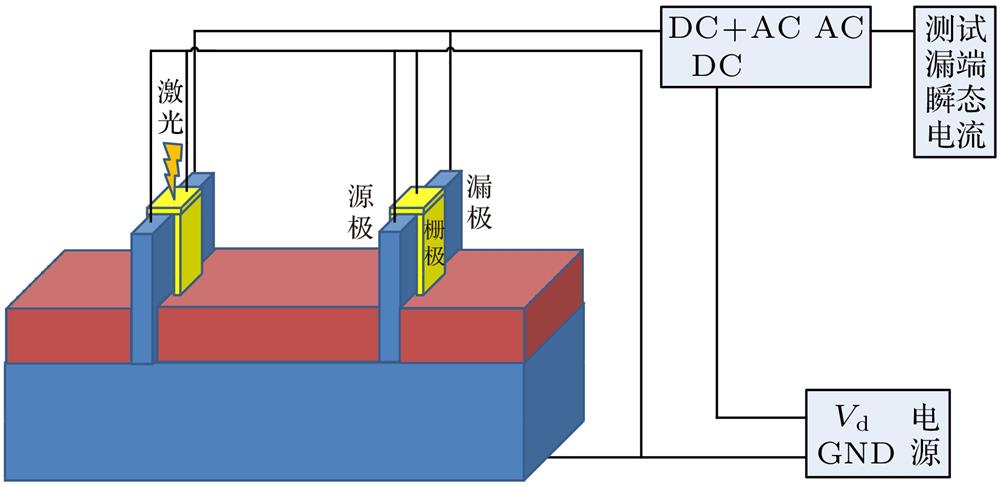
    Fig. 2. The circuit schematic of experience.
    Drain current transients for 4 fin FinFET of different gate length during the 5 nJ laser testing.
    Fig. 3. Drain current transients for 4 fin FinFET of different gate length during the 5 nJ laser testing.
    Drain charge collected for 4 fin FinFET of different gate length during the 5 nJ laser testing as a function of time.
    Fig. 4. Drain charge collected for 4 fin FinFET of different gate length during the 5 nJ laser testing as a function of time.
    Drain current transients for 2 fin FinFET of different gate length during the 5 nJ laser testing.
    Fig. 5. Drain current transients for 2 fin FinFET of different gate length during the 5 nJ laser testing.
    \begin{document}$ I_{\rm d}\text{-}V_{\rm g} $\end{document} for simulation single-fin FinFET and experimental 2 and 4 fins FinFET.
    Fig. 6. \begin{document}$ I_{\rm d}\text{-}V_{\rm g} $\end{document} for simulation single-fin FinFET and experimental 2 and 4 fins FinFET.
    Drain current transients for FinFET of different substrate thickness from TCAD simulation.
    Fig. 7. Drain current transients for FinFET of different substrate thickness from TCAD simulation.
    Drain current transients for FinFET of different gate length from TCAD simulation.
    Fig. 8. Drain current transients for FinFET of different gate length from TCAD simulation.
    Charge generation radial distribution of heavy ion
    Fig. 9. Charge generation radial distribution of heavy ion
    Temporary evolution of electronic density and electrostatic potential for a 30 nm FinFET.
    Fig. 10. Temporary evolution of electronic density and electrostatic potential for a 30 nm FinFET.
    Electronic density for FinFET of different gate length at 1.5 ns.
    Fig. 11. Electronic density for FinFET of different gate length at 1.5 ns.
    Drain current transient for 30 nm FinFET when heavy ion incident device with different radius.
    Fig. 12. Drain current transient for 30 nm FinFET when heavy ion incident device with different radius.
    Drain current transient for a FinFET when heavy ion incident at drain and gate.
    Fig. 13. Drain current transient for a FinFET when heavy ion incident at drain and gate.
    Chao Lu, Wei Chen, Yin-Hong Luo, Li-Li Ding, Xun Wang, Wen Zhao, Xiao-Qiang Guo, Sai Li. Effect of source-drain conduction in single-event transient on nanoscaled bulk fin field effect transistor[J]. Acta Physica Sinica, 2020, 69(8): 086101-1
    Download Citation