• Photonics Research
  • Vol. 10, Issue 4, 896 (2022)
Xipu Dong1, Jierong Cheng1、2、*, Yiwu Yuan1, Zhenyu Xing1, Fei Fan1, Xianghui Wang1, and Shengjiang Chang1、3
Author Affiliations
  • 1Institute of Modern Optics, Nankai University, Tianjin 300350, China
  • 2Tianjin Key Laboratory of Micro-scale Optical Information Science and Technology, Tianjin 300350, China
  • 3Tianjin Key Laboratory of Optoelectronic Sensor and Sensing Network Technology, Tianjin 300350, China
  • show less
    DOI: 10.1364/PRJ.438059 Cite this Article Set citation alerts
    Xipu Dong, Jierong Cheng, Yiwu Yuan, Zhenyu Xing, Fei Fan, Xianghui Wang, Shengjiang Chang. Arbitrary large-gradient wavefront shaping: from local phase modulation to nonlocal diffraction engineering[J]. Photonics Research, 2022, 10(4): 896 Copy Citation Text show less
    (a) Schematic of wavefront shaping through a metasurface. (b) Implementation of the desired continuous phase profile (solid curve) using the LPM method. The discretized phases are shown by the dots. Each of them is implemented by a subwavelength element shown below the phase curve. (c) Implementation of the desired continuous phase profile (solid curve) using the nLDM method. The desired phase profile is divided into several segments (shown by different colors) according to the 2π zones. Each phase segment is translated into a diffraction pattern and then implemented by a superwavelength-scale metagrating. (d), (e) The field distribution after the metasurface in the first 2π zone designed by the LPM method (d) and by the nLDM method (e).
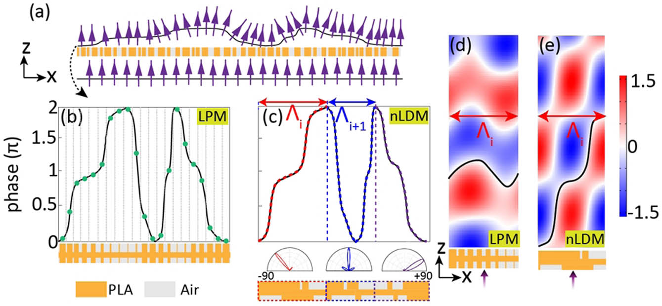
    Fig. 1. (a) Schematic of wavefront shaping through a metasurface. (b) Implementation of the desired continuous phase profile (solid curve) using the LPM method. The discretized phases are shown by the dots. Each of them is implemented by a subwavelength element shown below the phase curve. (c) Implementation of the desired continuous phase profile (solid curve) using the nLDM method. The desired phase profile is divided into several segments (shown by different colors) according to the 2π zones. Each phase segment is translated into a diffraction pattern and then implemented by a superwavelength-scale metagrating. (d), (e) The field distribution after the metasurface in the first 2π zone designed by the LPM method (d) and by the nLDM method (e).
    Metalenses for high-NA focusing with (a) a single focal spot and (b) four focal spots. The desired phase profiles of metalenses 1 and 2 folded within 2π are shown by the black curves in (c) and (d), respectively. The diffraction pattern of each 2π zone is shown by the histogram in (c) and (d), with the height of the bar indicating the diffraction efficiency and the color of the bar indicating the diffraction phase in each order. (e) The target diffraction patterns and the practical diffraction patterns of the optimized metagrating elements corresponding to four phase segments marked by the red curves in (c) and (d). The efficiency and phase in each diffraction order are shown by the height and color of the bar. The phase distributions after the optimized metagratings and the target phase segments are compared in (f)–(i).
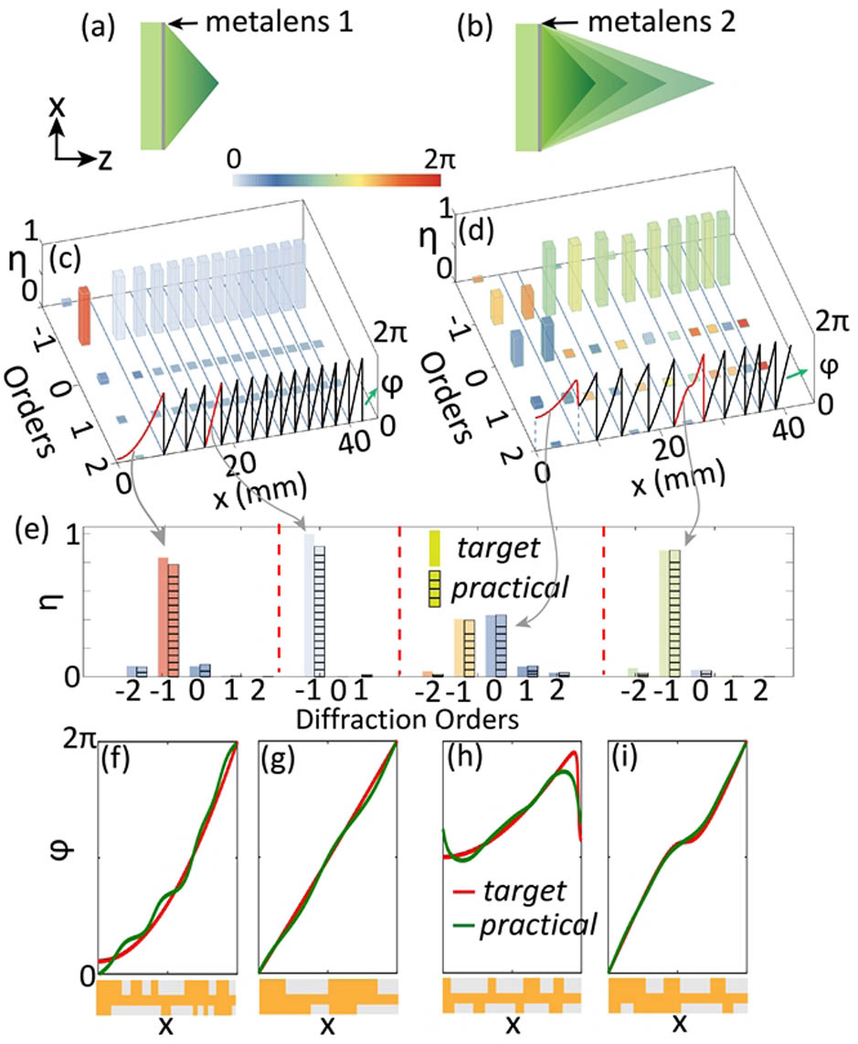
    Fig. 2. Metalenses for high-NA focusing with (a) a single focal spot and (b) four focal spots. The desired phase profiles of metalenses 1 and 2 folded within 2π are shown by the black curves in (c) and (d), respectively. The diffraction pattern of each 2π zone is shown by the histogram in (c) and (d), with the height of the bar indicating the diffraction efficiency and the color of the bar indicating the diffraction phase in each order. (e) The target diffraction patterns and the practical diffraction patterns of the optimized metagrating elements corresponding to four phase segments marked by the red curves in (c) and (d). The efficiency and phase in each diffraction order are shown by the height and color of the bar. The phase distributions after the optimized metagratings and the target phase segments are compared in (f)–(i).
    (a) Photograph of 3D-printed metalens 1 and its designed cross section. (b) Photograph of 3D-printed metalens 2 and its designed cross section. The segments analyzed in Fig. 2 are marked by the red boxes. (c) Experimental setup for testing the metalenses.
    Fig. 3. (a) Photograph of 3D-printed metalens 1 and its designed cross section. (b) Photograph of 3D-printed metalens 2 and its designed cross section. The segments analyzed in Fig. 2 are marked by the red boxes. (c) Experimental setup for testing the metalenses.
    (a) Simulated and (b) measured total electric field intensity distribution of metalens 1 in the xz plane. (c) Normalized intensity distribution along x in the focal plane. The simulated transverse field intensity and total intensity distribution are different due to the contribution of the longitudinal field component. The inset is the measured field distribution in the focal plane, showing a cylindrical focusing effect. (d) Simulated and (e) measured intensity distribution of metalens 2. (f) Intensity distribution along the optical axis.
    Fig. 4. (a) Simulated and (b) measured total electric field intensity distribution of metalens 1 in the xz plane. (c) Normalized intensity distribution along x in the focal plane. The simulated transverse field intensity and total intensity distribution are different due to the contribution of the longitudinal field component. The inset is the measured field distribution in the focal plane, showing a cylindrical focusing effect. (d) Simulated and (e) measured intensity distribution of metalens 2. (f) Intensity distribution along the optical axis.
    (a) Photograph of 3D-printed polarization-insensitive metalens 3 with NA=0.94. (b) −1st order diffraction efficiencies and phases of constituent segments in the metalens. The dotted lines are diffraction efficiencies η and star lines are diffraction phases ψ. Black ones are the target from Eq. (2), while green and orange ones are the practically optimized ones for TM and TE polarization, respectively. (c) Simulated and (d) measured intensity distribution in the focal plane. Polarization of the focus is superimposed in (c). (e), (f) Samples and measured images with different linewidths.
    Fig. 5. (a) Photograph of 3D-printed polarization-insensitive metalens 3 with NA=0.94. (b) 1st order diffraction efficiencies and phases of constituent segments in the metalens. The dotted lines are diffraction efficiencies η and star lines are diffraction phases ψ. Black ones are the target from Eq. (2), while green and orange ones are the practically optimized ones for TM and TE polarization, respectively. (c) Simulated and (d) measured intensity distribution in the focal plane. Polarization of the focus is superimposed in (c). (e), (f) Samples and measured images with different linewidths.
    (a) Target phase profile (black) of metalens 1 and the reproduced phase segments (red) by the optimized metagratings. (b) Summarized diffraction efficiencies and phases of the −1st order for all the segments in metalens 1. (c) Target phase profile (black) of metalens 2 and the reproduced phase segments (red) by the optimized metagratings. (d) Summarized diffraction efficiencies and phases of the −1st order for all the segments in metalens 2.
    Fig. 6. (a) Target phase profile (black) of metalens 1 and the reproduced phase segments (red) by the optimized metagratings. (b) Summarized diffraction efficiencies and phases of the 1st order for all the segments in metalens 1. (c) Target phase profile (black) of metalens 2 and the reproduced phase segments (red) by the optimized metagratings. (d) Summarized diffraction efficiencies and phases of the 1st order for all the segments in metalens 2.
    Detailed comparison of the target and reproduced phase segments of different shapes. (a) The first segment in Fig. 6(a). (b) The fourth segment in Fig. 6(a). (c), (d) The first segment in Fig. 6(c). The black lines are the target phase curves. The purple lines are the results of plane wave superposition in all the propagation orders. The purple dash line in (c) is the result of plane wave superposition in all the propagation orders and additional 8 evanescent orders. The green lines are the practical phases realized by the optimized metagratings.
    Fig. 7. Detailed comparison of the target and reproduced phase segments of different shapes. (a) The first segment in Fig. 6(a). (b) The fourth segment in Fig. 6(a). (c), (d) The first segment in Fig. 6(c). The black lines are the target phase curves. The purple lines are the results of plane wave superposition in all the propagation orders. The purple dash line in (c) is the result of plane wave superposition in all the propagation orders and additional 8 evanescent orders. The green lines are the practical phases realized by the optimized metagratings.
    (a) Transmission and phase response of subwavelength PLA elements with different duty cycles. The stars show eight elements with fixed phase difference of 0.25π to reproduce the phase profile of the metalens with NA of 0.94. The inset is one element. (b) Simulated normalized intensity distributions on the focal plane. The black line is for the LPM-based metalens and the red line is for the nLDM-based metalens 1 in the main text. (c) Geometries of the nLDM-based metalens 1 and the LPM-based metalens. (d)–(f) The same information as (a)–(c) for metalenses made of silicon.
    Fig. 8. (a) Transmission and phase response of subwavelength PLA elements with different duty cycles. The stars show eight elements with fixed phase difference of 0.25π to reproduce the phase profile of the metalens with NA of 0.94. The inset is one element. (b) Simulated normalized intensity distributions on the focal plane. The black line is for the LPM-based metalens and the red line is for the nLDM-based metalens 1 in the main text. (c) Geometries of the nLDM-based metalens 1 and the LPM-based metalens. (d)–(f) The same information as (a)–(c) for metalenses made of silicon.
    Xipu Dong, Jierong Cheng, Yiwu Yuan, Zhenyu Xing, Fei Fan, Xianghui Wang, Shengjiang Chang. Arbitrary large-gradient wavefront shaping: from local phase modulation to nonlocal diffraction engineering[J]. Photonics Research, 2022, 10(4): 896
    Download Citation