
Xipu Dong, Jierong Cheng, Yiwu Yuan, Zhenyu Xing, Fei Fan, Xianghui Wang, Shengjiang Chang, "Arbitrary large-gradient wavefront shaping: from local phase modulation to nonlocal diffraction engineering," Photonics Res. 10, 896 (2022)
- Photonics Research
- Vol. 10, Issue 4, 896 (2022)
Abstract
1. INTRODUCTION
In the past decades, remarkable progress in metasurfaces has revolutionized wavefront shaping in a planar, miniaturized, and multifunctional way, which is enabled not by the phase accumulation during the propagation path but by the phase discontinuity at the interfacial boundary [1–3]. The abrupt phase discontinuity is encoded in elaborately designed subwavelength elements through various types of interaction with the incident light, such as electric and magnetic resonances [4,5], waveguide effect [6,7], and Pancharatnam–Berry phase [8]. The implementation of a continuous phase profile is through subwavelength discretization, and each element is only responsible for local phase modulation over its occupied subwavelength area. We name this type of wavefront shaping as local phase modulation (LPM), which is widely used in metasurface-based beam focusing [9–11], polarization control [12], holographic imaging [13,14], and so on.
Despite its remarkable success in wavefront control, LPM poses some limitations to metasurfaces. First, the phase response of each element is approximated by that of the element in locally periodic environment. This assumption fundamentally limits the application scenarios of LPM to slowly varying wavefronts. It further limits the material of metasurfaces to be high-index dielectrics or metals [15] as strong field localization is needed to minimize the coupling of adjacent elements in the aperiodic array. More importantly, LPM overlooks the impedance mismatch between the input and output beams, which inherently leads to increasingly strong parasitic scattering into undesired directions with the increase of the phase gradient [16]. Large-gradient phase profile is highly required in implementing tight focusing, beam multiplexing, or more complex wavefront shaping. In these cases, LPM-based metasurfaces become inefficient [6,17,18].
To circumvent these problems, metagratings [19] with superwavelength periods are proposed for near-perfect large-angle deflection by gathering energy into the first diffraction order (blazed diffraction) [20–25]. As constitutive elements of metasurfaces, metagratings with different periods and internal geometries are then combined for broad-angle beam scattering [26] and for metalenses with numerical aperture (NA) as high as 0.99 [27,28]. Each metagrating efficiently reroutes the beam following the ray path in geometric optics through efficient blazed diffraction.
Sign up for Photonics Research TOC. Get the latest issue of Photonics Research delivered right to you!Sign up now
However, the diffraction phase of metagratings is not studied yet. In fact, precise control of the diffraction phase is as important as maximization of the diffraction efficiency, as the incoming beam should be piecewise diffracted and constructively superimposed to build the desired wavefront. Furthermore, an arbitrary nonlinear-shaped large-gradient wavefront manipulation may not require piecewise blazed diffraction but other diffraction patterns. One should flexibly control the energy distribution among different orders and simultaneously control the diffraction phases so as to accurately reproduce a piece of arbitrary-shaped phase profile.
In this work, we propose a general mechanism for arbitrary large-gradient wavefront shaping by controlling a full set of diffraction parameters (direction, efficiency, and phase of each order) of superwavelength elements. The desired phase profile is cut into segments according to
As proof of the concept, we theoretically design and experimentally study high-NA cylindrical metalenses and 3D metalenses based on nLDM in the terahertz (THz) band. They show diffraction-limited focal spots, high efficiency, and subwavelength imaging resolution. As compared to LPM, nLDM serves as a better choice for large-gradient wavefront transformation. It brings additional merits of flexible choice of abundant dielectric materials and various processing methods, as strong field localization is not required. The method is general and can be extended for wavefront shaping at other frequencies.
2. NONLOCAL DIFFRACTION METHOD FOR LARGE-GRADIENT WAVEFRONT SHAPING
Figure 1(a) shows an arbitrary wavefront shaping over a metasurface. The tangential field before and after the metasurface can be represented by
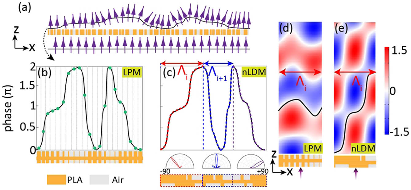
Figure 1.(a) Schematic of wavefront shaping through a metasurface. (b) Implementation of the desired continuous phase profile (solid curve) using the LPM method. The discretized phases are shown by the dots. Each of them is implemented by a subwavelength element shown below the phase curve. (c) Implementation of the desired continuous phase profile (solid curve) using the nLDM method. The desired phase profile is divided into several segments (shown by different colors) according to the
In contrast, nLDM divides the continuous phase curve into several segments, which can be described as
There is no discritization error as compared to Fig. 1(b). The starting point and ending point (
In order to meet so many diffraction requirements, we combine an optimization algorithm with electromagnetic simulation to find the metagrating quickly and automatically. We use the gradient descent optimization function fmincon in MATLAB and rigorously coupled wave analysis (RCWA) to approach the ideal diffraction by minimizing the following cost function:
Lastly, the metagrating should have enough degree of freedom so as to achieve different types of diffraction patterns. Here it is composed of bilayer one-dimensional ridges [Fig. 1(c)] made of polymer polylactic acid (PLA), whose refractive index is 1.57 at the target frequency 0.14 THz. Our previous study has proven the success of this type of metagrating for efficient large-angle diffraction [24,31], beam splitting [29], and asymmetric diffraction [32]. To ensure a planar profile of the metasurface, the thickness of each layer is not tuned. Throughout the manuscript, the ridges in the incident side are 2.0 mm thick, the slab is 2.1 mm thick, and the ridges in the transmission side are 3.1 mm thick if not mentioned.
As an example, we implement the red phase segment in Fig. 1(c) using LPM and nLDM at 0.14 THz. The length of this segment is
3. HIGH-NA CYLINDRICAL METALENSES
As proofs of the concept, we design two high-NA cylindrical metalenses with one and four focal spots, respectively, using the nLDM method as shown in Figs. 2(a) and 2(b). The diameter of both metalenses is 82 mm (
![]()
Figure 2.Metalenses for high-NA focusing with (a) a single focal spot and (b) four focal spots. The desired phase profiles of metalenses 1 and 2 folded within
Next, using RCWA and the gradient descent optimization algorithm, we successfully find all the metagratings to reproduce the target diffraction patterns with
The two metalenses are then 3D printed and experimentally tested. The metalenses are fabricated by a commercial 3D printer (Raise3D N2) using a fused-deposition modeling method. The diameter of the nozzle is 200 μm. The base plate and printing nozzle are set to 60°C and 215°C, respectively. The printing speed has a constant value of 60 mm/s. The metalens is piled up layer by layer along the y direction. Printing of each metalens takes 10 h approximately. The designed and 3D-printed metalenses are shown in Figs. 3(a) and 3(b), and the experiment setup in Fig. 3(c) is used to characterize the focusing performance. The source is a continuous-wave IMPATT diode at 0.14 THz. The beam is collimated by a Teflon convex lens with a focal length of 200 mm and a diameter of 4 inches. A half-wave plate is used to convert the polarization from the y to the x direction, so that the electric field is perpendicular to the ridges of cylindrical metalenses. To measure the field distribution after the metalens, a Schottky diode detector with an iris (diameter of 1 mm) is mounted on a three-dimensional translation stage and scanned with the step of 0.25 mm in the x, y, and z directions. For terahertz imaging, the imaging sample is mounted on the translation stage for scanning along the x and y directions in the focal plane. The detector is fixed at the optical axis after the sample for detection. A lock-in amplifier is connected to the source and the detector for modulation and lock-in detection.
![]()
Figure 3.(a) Photograph of 3D-printed metalens 1 and its designed cross section. (b) Photograph of 3D-printed metalens 2 and its designed cross section. The segments analyzed in Fig.
For better comparison, simulations of the two metalenses are carried out in Lumerical FDTD Solutions with the Gaussian beam source polarized along the
![]()
Figure 4.(a) Simulated and (b) measured total electric field intensity distribution of metalens 1 in the
In addition, the simulated focusing efficiency of 52% of the metalens 1 seems not a significant improvement if compared with some state-of-the-art metalenses in the optical region with similar NA designed using the LPM method [6,35,36]. However, they are all made of high-index dielectric on low-index substrate with very large aspect ratio, which is challenging at the terahertz band [10]. If we redesign the metalens 1 using the LPM method, the focusing efficiency is only 25.2%. So the 52% focusing efficiency does indicate the effectiveness of nLDM in boosting the performance of high-NA metalenses. In addition, the focusing efficiency can be improved to 59% and 71% in silicon-on-silicon metalenses and silicon-on-
The simulated and measured field distributions through metalens 2 are shown in Figs. 4(d) and 4(e), which show excellent coincidence. Figure 4(f) plots the intensity along the optical axis, where four peaks can be identified. However, since the second and third peaks are very close, they cannot be distinguished through the measurement. Still the general trend and the relative intensity of the foci agree well with the simulation.
4. 3D TIGHT FOCUSING AND IMAGING
To further generalize the functionality from 2D focusing into full-space 3D focusing, the cylindrical metalens can simply be rotated around its center forming the concentric ring metalens. To ensure good quality of 3D tight focusing in the concentric ring metalens with linearly polarized excitation, it is necessary to have polarization-insensitive 2D metagratings, meaning the same diffraction patterns for both TE and TM polarization states. Since the metalens 1 is only optimized for TM polarization, we redesigned all the 14 segments in Fig. 2(c) by minimizing the cost function in both polarization states as
![]()
Figure 5.(a) Photograph of 3D-printed polarization-insensitive metalens 3 with
To characterize the imaging performance of the metalens, we mount the imaging sample on a translation stage and scan it in the focal plane of the 3D metalens. A Schottky detector with a pin hole is fixed behind the sample to record the field distribution. The sample in Fig. 5(e) is a metallic sheet with etched “NK” letters whose linewidth is 2 mm. The detected intensity distribution can well resolve the letters. Next, we change the imaging sample into a resolution chart in Fig. 5(f). From left to right, the width of the bar is 2.0 mm, 1.8 mm, 1.4 mm, 0.9 mm, and 0.6 mm. The detected image shows a resolution of 1.4 mm, which is
5. DISCUSSION AND CONCLUSION
We notice that each segment is designed and optimized in a periodic environment, while the whole device is aperiodic. This will inevitably bring some error. If we take the segmented metalens 1 as an initial solution and further numerically optimize the entire structure, the focusing efficiency is slightly boosted from 52% to 60%, indicating the rationality of the periodic assumption. This assumption now is in the superwavelength scale, therefore being better satisfied than the subwavelength periodic assumption in the LPM. For the case when the phase segment is drastically different from the neighboring ones, one can merge it to the neighboring one to form a larger segment. It will make the wavefront shaping more accurate. Nevertheless, the periodic assumption makes it possible to translate a continuous phase segment into a few discrete diffraction coefficients, which significantly reduce the information dimension, and simplify the optimization.
We know the LPM-based metasurface can be readily generated regardless of the device size once some basic subwavelength elements are found. In the nLDM, the optimization time will increase linearly with the scale of the metasurface, since each segment is optimized separately. However, the average optimization time for each segment is around 7 s. It is not a problem to deal with large-scale devices. In contrast, global optimization of the full metalens, though being a good solution to push the NA and to improve the efficiency [38–41], needs extensive computational resources and severely limits the scale of the devices. The proposed nLDM strategy is much more time-efficient in design and provides rich physical insights into the wavefront transformation.
Finally, the nonlocal diffraction engineering method is general enough to be applied at other frequency bands. When working at higher frequencies, it is possible to etch both sides of the glass plate or to build bi-layer photoresist structures similar to the one demonstrated here. Instead, one can simply choose high-index dielectric monolayer structures for nonlocal diffraction engineering. In Appendix B, we also give a monolayer metalens made of silicon with improved efficiency when designed using the nonlocal diffraction engineering, which can be scaled to optical frequencies and fabricated by conventional lithography techniques.
To summarize, we demonstrate that arbitrary large-gradient wavefront shaping can be accurately and effectively achieved from the nonlocal diffraction engineering of the superwavelength-scale metagratings. Different from the local phase modulation where each phase point corresponds to a subwavelength element, the proposed method here establishes correlation between the phase segments and the diffraction patterns, and further finds the proper metagrating geometry to fulfill the diffraction properties including diffraction angles, diffraction efficiencies, and diffraction phases. High-NA cylindrical metalenses composed of a series of metagratings are designed and experimentally tested, showing the effectiveness and flexibility of this method for arbitrary 2D wavefront shaping. The design is further extended to 3D metalenses by utilizing polarization-insensitive metagratings, whose application in high-resolution imaging is well characterized. These findings indicate that the nonlocal diffraction engineering offers a new perspective on beam transformation over metasurface devices, well suited for large-gradient cases.
APPENDIX A: PHASE PROFILE REPRODUCTION BASED ON THE nLDM
As aforementioned, metalens 1 contains 14 metagrating segments, and metalens 2 contains 11 metagrating segments. In order to show the accuracy of the optimized metagratings, the phase profile after each metagrating is shown piecewise on top of the ideal phase profile in Figs.
![]()
Figure 6.(a) Target phase profile (black) of metalens 1 and the reproduced phase segments (red) by the optimized metagratings. (b) Summarized diffraction efficiencies and phases of the
![]()
Figure 7.Detailed comparison of the target and reproduced phase segments of different shapes. (a) The first segment in Fig.
The practical phases realized by the optimized metagratings are shown by the green curves. The optimization brings some error to all the three phase segments, and it is more pronounced in the nonlinear shaped ones in Figs.
APPENDIX B: COMPARISON OF LPM- AND nLDM-BASED METALENSES MADE OF DIFFERENT DIELECTRICS
Here we compare the focusing performance of the same metalens designed using the LPM and nLDM methods. In order to show that the nLDM is better than LPM no matter of the metalens material, we carry out this comparison in low-index metalenses made of PLA and in high-index metalenses made of silicon, respectively.
The performance of the nLDM-based metalens made of PLA has been studied. Here we show the design and response of the LPM-based metalens made of PLA. Figure
![]()
Figure 8.(a) Transmission and phase response of subwavelength PLA elements with different duty cycles. The stars show eight elements with fixed phase difference of
Similarly, two metalenses made of silicon (refractive index of 3.5) are designed by the LPM and nLDM methods, respectively. The thicknesses of the silicon grating ridges and the silicon substrate are chosen as
References
[1] H. Chen, A. J. Taylor, N. Yu. A review of metasurfaces: physics and applications. Rep. Prog. Phys., 79, 076401(2016).
[2] S. Chang, X. Guo, X. Ni. Optical metasurfaces: progress and applications. Annu. Rev. Mater. Res., 48, 279-302(2018).
[3] F. Ding, A. Pors, S. I. Bozhevolnyi. Gradient metasurfaces: a review of fundamentals and applications. Rep. Prog. Phys., 81, 026401(2018).
[4] M. Decker, I. Staude, M. Falkner, J. Dominguez, D. N. Neshev, I. Brener, T. Pertsch, Y. S. Kivshar. High-efficiency dielectric Huygens’ surfaces. Adv. Opt. Mater., 3, 813-820(2015).
[5] J. Cheng, D. Ansari-Oghol-Beig, H. Mosallaei. Wave manipulation with designer dielectric metasurfaces. Opt. Lett., 39, 6285-6288(2014).
[6] A. Arbabi, E. Arbabi, S. M. Kamali, Y. Horie, S. Han, A. Faraon. Miniature optical planar camera based on a wide-angle metasurface doublet corrected for monochromatic aberrations. Nat. Commun., 7, 13682(2016).
[7] Z. Fan, Z. Shao, M. Xie, X. Pang, W. Ruan, F. Zhao, Y. Chen, S. Yu, J. Dong. Silicon nitride metalenses for close-to-one numerical aperture and wide-angle visible imaging. Phys. Rev. Appl., 10, 014005(2018).
[8] M. Khorasaninejad, W. Chen, R. Devlin, J. Oh, A. Y. Zhu, F. Capasso. Metalenses at visible wavelengths: diffraction limited focusing and subwavelength resolution imaging. Science, 352, 1190-1194(2016).
[9] M. Khorasaninejad, F. Capasso. Metalenses: versatile multifunctional photonic components. Science, 358, eaam8100(2017).
[10] H. Chen, Z. Wu, Z. Li, Z. Luo, X. Jiang, Z. Wen, L. Zhu, X. Zhou, X. H. Li, Z. Shang, Z. Zhang, K. Zhang, G. Liang, S. Jiang, L. Du, G. Chen. Sub-wavelength tight-focusing of terahertz waves by polarization-independent high numerical-aperture dielectric metalens. Opt. Express, 26, 29817-29825(2018).
[11] H. Zhang, X. Zhang, Q. Xu, C. Tian, Q. Wang, Y. Xu, Y. Li, J. Gu, Z. Tian, C. Ouyang, X. Zhang, C. Hu, J. Han, W. Zhang. High-efficiency dielectric metasurfaces for polarization-dependent terahertz wavefront manipulation. Adv. Opt. Mater., 6, 1700773(2018).
[12] X. Cai, R. Tang, H. Zhou, Q. Li, S. Ma, D. Wang, T. Liu, X. Ling, W. Tan, Q. He, S. Xiao, L. Zhou. Dynamically controlling terahertz wavefronts with cascaded metasurfaces. Adv. Photonics, 3, 036003(2021).
[13] G. Y. Lee, J. Sung, B. Lee. Recent advances in metasurface hologram technologies. ETRI J., 41, 10-22(2019).
[14] G. Zheng, H. Mühlenbernd, M. Kenney, G. Li, T. Zentgraf, S. Zhang. Metasurface holograms reaching 80% efficiency. Nat. Nanotechnol., 10, 308-312(2015).
[15] J. Yang, J. A. Fan. Analysis of material selection on dielectric metasurface performance. Opt. Express, 25, 23899-23909(2017).
[16] V. S. Asadchy, M. Albooyeh, S. N. Tcvetkova, A. Díaz-Rubio, Y. Ra’di, S. A. Tretyakov. Perfect control of reflection and refraction using spatially dispersive metasurfaces. Phys. Rev. B, 94, 075142(2016).
[17] H. Liang, A. Martins, B.-H. V. Borges, J. Zhou, E. R. Martins, J. Li, T. F. Krauss. High performance metalenses: numerical aperture, aberrations, chromaticity, and trade-offs. Optica, 6, 1461-1470(2019).
[18] V. S. Asadchy, A. Wickberg, A. Díaz-Rubio, M. Wegener. Eliminating scattering loss in anomalously reflecting optical metasurfaces. ACS Photonics, 4, 1264-1270(2017).
[19] Y. Ra’di, D. L. Sounas, A. Alu. Metagratings: beyond the limits of graded metasurfaces for wave front control. Phys. Rev. Lett., 119, 067404(2017).
[20] A. Díaz-Rubio, V. S. Asadchy, A. Elsakka, S. A. Tretyakov. From the generalized reflection law to the realization of perfect anomalous reflectors. Sci. Adv., 3, e1602714(2017).
[21] A. M. H. Wong, G. V. Eleftheriades. Perfect anomalous reflection with a bipartite Huygens’ metasurface. Phys. Rev. X, 8, 011036(2018).
[22] D. Sell, J. Yang, S. Doshay, R. Yang, J. A. Fan. Large-angle, multifunctional metagratings based on freeform multimode geometries. Nano Lett., 17, 3752-3757(2017).
[23] Z. Fan, M. R. Shcherbakov, M. Allen, J. Allen, B. Wenner, G. Shvets. Perfect diffraction with multiresonant bianisotropic metagratings. ACS Photonics, 5, 4303-4311(2018).
[24] X. Dong, J. Cheng, F. Fan, S. Chang. Low-index second-order metagratings for large-angle anomalous reflection. Opt. Lett., 44, 939-942(2019).
[25] Z. Zhang, M. Kang, X. Zhang, X. Feng, Y. Xu, X. Chen, H. Zhang, Q. Xu, Z. Tian, W. Zhang, A. Krasnok, J. Han, A. Alù. Coherent perfect diffraction in metagratings. Adv. Mater., 32, 2002341(2020).
[26] V. Neder, Y. Ra’Di, A. Alù, A. Polman. Combined metagratings for efficient broad-angle scattering metasurface. ACS Photonics, 6, 1010-1017(2019).
[27] R. Paniagua-Dominguez, Y. F. Yu, E. Khaidarov, S. Choi, V. Leong, R. M. Bakker, X. Liang, Y. H. Fu, V. Valuckas, L. A. Krivitsky, A. I. Kuznetsov. A metalens with a near-unity numerical aperture. Nano Lett., 18, 2124-2132(2018).
[28] M. Kang, Y. Ra’di, D. Farfan, A. Alù. Efficient focusing with large numerical aperture using a hybrid metalens. Phys. Rev. Appl., 13, 044016(2020).
[29] X. Dong, J. Cheng, F. Fan, X. Wang, S. Chang. Efficient wide-band large-angle refraction and splitting of a terahertz beam by low-index 3D-printed bilayer metagratings. Phys. Rev. Appl., 14, 014064(2020).
[30] S. Larouche, D. R. Smith. Reconciliation of generalized refraction with diffraction theory. Opt. Lett., 37, 2391-2393(2012).
[31] X. Dong, J. Cheng, F. Fan, Z. Zhang, Y. Liu, X. Wang, S. Chang. Extremely large-angle beam deflection based on low-index sparse dielectric metagratings. J. Phys. D, 53, 245101(2020).
[32] X. Dong, J. Cheng, Y. Yuan, F. Fan, X. Wang, S. Chang. An efficient bi-functional metagrating via asymmetric diffraction of terahertz beams. IEEE Photonics Technol. Lett., 33, 441-444(2021).
[33] F. Zhang, H. Yu, J. Fang, M. Zhang, S. Chen, J. Wang, A. He, J. Chen. Efficient generation and tight focusing of radially polarized beam from linearly polarized beam with all-dielectric metasurface. Opt. Express, 24, 6656-6664(2016).
[34] Z. Wang, Q. Li, F. Yan. A high numerical aperture terahertz all-silicon metalens with sub-diffraction focus and long depth of focus. J. Phys. D, 54, 085103(2020).
[35] H. Liang, Q. Lin, X. Xie, Q. Sun, Y. Wang, L. Zhou, L. Liu, X. Yu, J. Zhou, T. F. Krauss, J. Li. Ultrahigh numerical aperture metalens at visible wavelengths. Nano Lett., 18, 4460-4466(2018).
[36] S. J. Byrnes, A. Lenef, F. Aieta, F. Capasso. Designing large, high-efficiency, high-numerical-aperture, transmissive meta-lenses for visible light. Opt. Express, 24, 5110-5124(2016).
[37] E. Noponen, J. Turunen, A. Vasara. Electromagnetic theory and design of diffractive-lens arrays. J. Opt. Soc. Am. A, 10, 434-443(1993).
[38] S. Banerji, B. Sensale-Rodriguez. A computational design framework for efficient, fabrication error-tolerant, planar THz diffractive optical elements. Sci. Rep., 9, 5801(2019).
[39] M. Mansouree, A. McClung, S. Samudrala, A. Arbabi. Large-scale parametrized metasurface design using adjoint optimization. ACS Photonics, 8, 455-463(2021).
[40] Z. Lin, B. Groever, F. Capasso, A. W. Rodriguez, M. Lončar. Topology-optimized multilayered metaoptics. Phys. Rev. Appl., 9, 044030(2018).
[41] H. Chung, O. D. Miller. High-NA achromatic metalenses by inverse design. Opt. Express, 28, 6945-6965(2020).


Set citation alerts for the article
Please enter your email address

© Copyright 2018-2021 | Chinese Laser Press. All Rights Reserved 沪ICP备15018463号-20