• Photonics Research
  • Vol. 6, Issue 1, 47 (2018)
Fengyuan Gan1、2, Chengwei Sun1, Hongyun Li1, Qihuang Gong1、2, and Jianjun Chen1、2、*
Author Affiliations
  • 1State Key Laboratory for Mesoscopic Physics, Collaborative Innovation Center of Quantum Matter, Department of Physics, Peking University, Beijing 100871, China
  • 2Collaborative Innovation Center of Extreme Optics, Shanxi University, Taiyuan 030006, China
  • show less
    DOI: 10.1364/PRJ.6.000047 Cite this Article Set citation alerts
    Fengyuan Gan, Chengwei Sun, Hongyun Li, Qihuang Gong, Jianjun Chen. On-chip polarization splitter based on a multimode plasmonic waveguide[J]. Photonics Research, 2018, 6(1): 47 Copy Citation Text show less
    (a) Schematic and geometrical parameters of the multimode plasmonic waveguide. Power flow distributions of the (b) symmetric waveguide mode and (c) antisymmetric waveguide mode for w=700 nm, h=400 nm, d=400 nm, θ=16°, t=200 nm, and r=5 nm. The green arrows denote the vectors of the electric field. (d) Effective refractive indices, (e) propagation lengths, and (f) field confinements of the symmetric (black lines) as well as antisymmetric (red lines) SPP waveguide modes varying with wavelengths. The green dashed line in (d) denotes the effective refractive indices of the SPP mode on the flat metal surface.
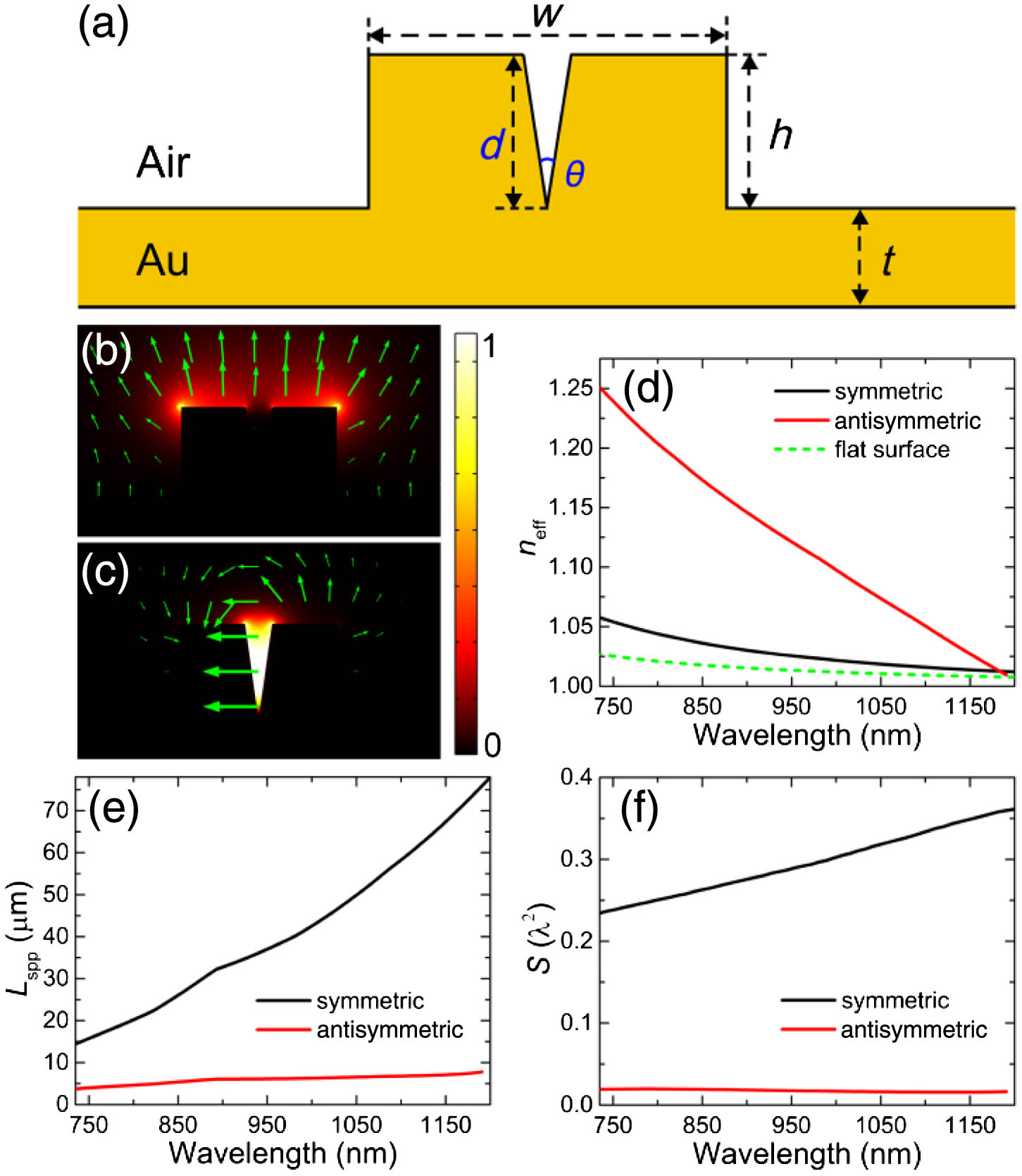
    Fig. 1. (a) Schematic and geometrical parameters of the multimode plasmonic waveguide. Power flow distributions of the (b) symmetric waveguide mode and (c) antisymmetric waveguide mode for w=700  nm, h=400  nm, d=400  nm, θ=16°, t=200  nm, and r=5  nm. The green arrows denote the vectors of the electric field. (d) Effective refractive indices, (e) propagation lengths, and (f) field confinements of the symmetric (black lines) as well as antisymmetric (red lines) SPP waveguide modes varying with wavelengths. The green dashed line in (d) denotes the effective refractive indices of the SPP mode on the flat metal surface.
    (a) Schematic of the bending multimode plasmonic waveguide. (b) Transmittances of the symmetric (dashed lines) and antisymmetric (solid lines) SPP waveguide modes passing through the bending waveguide at different bending radii and bending angles (λ=900 nm). Power flow distributions of the (c) symmetric and (d) antisymmetric waveguide modes at R=2 μm and α=30°.
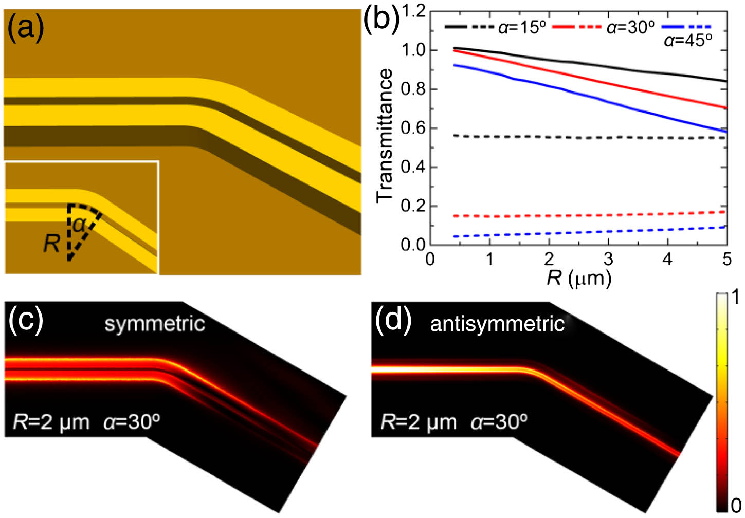
    Fig. 2. (a) Schematic of the bending multimode plasmonic waveguide. (b) Transmittances of the symmetric (dashed lines) and antisymmetric (solid lines) SPP waveguide modes passing through the bending waveguide at different bending radii and bending angles (λ=900  nm). Power flow distributions of the (c) symmetric and (d) antisymmetric waveguide modes at R=2  μm and α=30°.
    (a) Schematic and (b) top view of the proposed PBS. Power flow distributions of the (c) symmetric and (d) antisymmetric waveguide modes at λ=900 nm. Normalized output powers of the (e) symmetric and (f) antisymmetric waveguide modes at different wavelengths in the simulation.
    Fig. 3. (a) Schematic and (b) top view of the proposed PBS. Power flow distributions of the (c) symmetric and (d) antisymmetric waveguide modes at λ=900  nm. Normalized output powers of the (e) symmetric and (f) antisymmetric waveguide modes at different wavelengths in the simulation.
    (a) SEM image of the fabricated structures. (b) Cross-sectional SEM image of the multimode plasmonic waveguide. CMOS captured pictures under (c), (e), (g) p-polarized and (d), (f), (h) s-polarized incident light at different wavelengths. The red dashed rectangles in (c)−(h) denote the decoupling gratings.
    Fig. 4. (a) SEM image of the fabricated structures. (b) Cross-sectional SEM image of the multimode plasmonic waveguide. CMOS captured pictures under (c), (e), (g) p-polarized and (d), (f), (h) s-polarized incident light at different wavelengths. The red dashed rectangles in (c)−(h) denote the decoupling gratings.
    Measured normalized scattered powers under (a) p-polarized and (b) s-polarized incident light at different wavelengths. (c) Power flow distribution of the higher-order mode at λ=830 nm. The green arrows denote the vectors of the electric field. (d) Effective indices of the symmetric (black line), antisymmtric (red line) and higher-order (blue line) modes at different wavelengths. The green dashed line in (d) shows the effective indices of the SPP mode on the flat metal surface.
    Fig. 5. Measured normalized scattered powers under (a) p-polarized and (b) s-polarized incident light at different wavelengths. (c) Power flow distribution of the higher-order mode at λ=830  nm. The green arrows denote the vectors of the electric field. (d) Effective indices of the symmetric (black line), antisymmtric (red line) and higher-order (blue line) modes at different wavelengths. The green dashed line in (d) shows the effective indices of the SPP mode on the flat metal surface.
    Fengyuan Gan, Chengwei Sun, Hongyun Li, Qihuang Gong, Jianjun Chen. On-chip polarization splitter based on a multimode plasmonic waveguide[J]. Photonics Research, 2018, 6(1): 47
    Download Citation