
Hongwei Gao, George F. R. Chen, Peng Xing, Ju Won Choi, Dawn T. H. Tan. 3D printed on-chip microtoroid resonators and nested spiral photonic devices[J]. Photonics Research, 2021, 9(9): 1803
- Photonics Research
- Vol. 9, Issue 9, 1803 (2021)
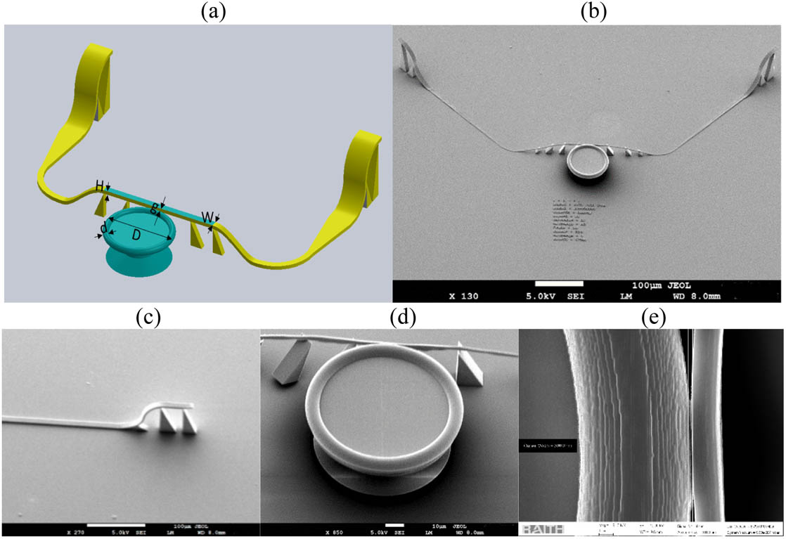
Fig. 1. (a) Schematic and (b) SEM image of the fabricated integrated microtoroid-waveguide system; principal diameter D = 88 μm d = 8 μm g = 300 nm W = 2 μm H = 2 μm
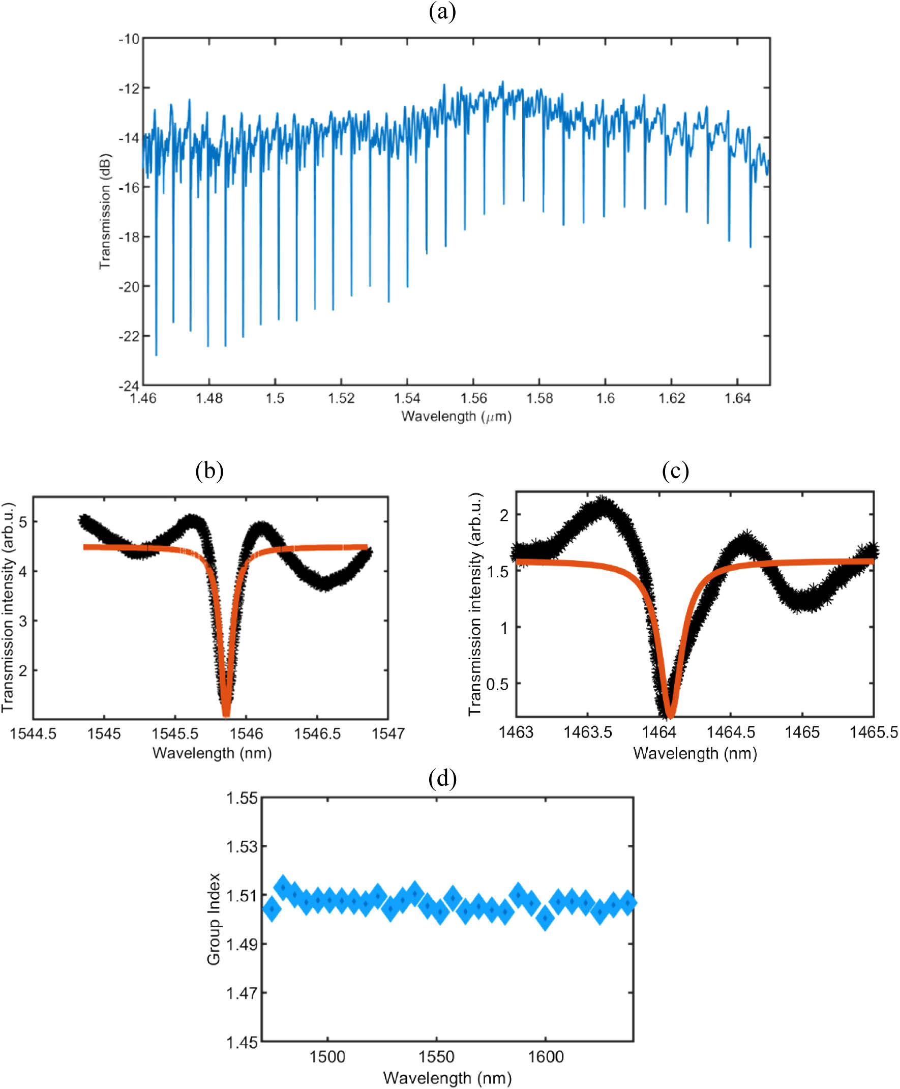
Fig. 2. (a) Transmission spectrum of microtoroid resonator. Major diameter is 80 μm, minor diameter is 8 μm, and gap is 300 nm. (b) Lorentzian fitting of a single resonance at 1545.8 nm; (c) Lorentzian fitting of a single resonance at 1464.1 nm; (d) group index as a function of wavelength.
Fig. 3. (a) Simulated transmission spectrum of microtoroid resonator. The major and minor diameters are 80 μm and 8 μm, respectively, and the gap is 300 nm. (b) Simulated mode profile at 1545.78 nm (on-resonance) and (c) at 1549.3 nm (off-resonance).
Fig. 4. SEM images of coupling region between the microtoroid and coupling waveguide with a gap of (a) 200 nm; (b) 300 nm; and (c) 400 nm; (d) measured transmission spectra of the microtoroid-waveguide with gaps of 200 nm (blue line), 300 nm (red line), and 400 nm (yellow line); (e) simulated transmission spectra of microtoroid-waveguide with gaps of 200 nm (blue line), 300 nm (red line), and 400 nm (yellow line).
Fig. 5. (a) SEM image of nested double-spiral waveguide; scale bar is 100 μm; (b) magnified view of the spiral region; scale bar is 10 μm; (c) input and output waveguide coupler; scale bar is 10 μm; (d) transmission spectrum of the nested double-spiral waveguide.
Fig. 6. High-speed testing setup using 30 Gb/s NRZ data and 28 Gb/s PAM4 data.
Fig. 7. (a) Plot of − log ( BER )

Set citation alerts for the article
Please enter your email address
© Copyright 2018-2021 | Chinese Laser Press. All Rights Reserved 沪ICP备15018463号-20