
Hongwei Gao, George F. R. Chen, Peng Xing, Ju Won Choi, Dawn T. H. Tan. 3D printed on-chip microtoroid resonators and nested spiral photonic devices[J]. Photonics Research, 2021, 9(9): 1803
- Photonics Research
- Vol. 9, Issue 9, 1803 (2021)
Abstract
1. INTRODUCTION
Optical resonators of various configurations are areas of active research. Their applications are plentiful and diverse, including quantum information processing [1–6], nonlinear optics [7,8], lasing [9], optical sensing [10–14], and mechanics [15–19]. Resonators greatly enhance the extent of light–matter interaction, reducing operating powers and/or device footprints. Within integrated optics, microring and microdisk resonators are the most prolific types of optical resonators, owing to their ease of integration in photonic light-wave circuits. Though microsphere and microtoroid resonators have been shown to have high quality factors, they are less commonly deployed. Compared to microsphere resonators, coupling to microtoroid resonators is more challenging. The latter’s optical mode is confined in a relatively small toroidal area, and the azimuthal expansion of the mode is significantly smaller. The width of the effective coupling area is within the minor diameter of the toroid. Consequently, small changes in height and horizontal position of the coupler relative to the microtoroid can completely quench the light coupled to the resonator.
Part of the challenge in microtoroid resonators is the coupling mechanism. Coupling to the resonator is usually achieved with phase- and mode-matched power exchange between the resonator modes and the guided wave propagating in a specially engineered coupler (a waveguide or a prism). In general, the nonintegrated coupler and whispering gallery mode (WGM) resonator are usually two independent elements. Coupling may be achieved using a nonintegrated tapered fiber. Typically, a nonintegrated tapered fiber needs to be positioned with high spatial precision (tens to hundreds of nanometers) next to the resonator, at a separation distance conducive to optimal fiber-resonator coupling. In addition, the nonintegrated fiber or specially engineered couplers present some packaging difficulties from the standpoint of photonic integrated circuits. Fabrication-wise, microtoroids utilize a multistep process. Silica microtoroids, for example, require a lithographic step followed by a buffered oxide etch to define the core of the microtoroid. An isotropic dry etch is then applied to release part of the silica from the silicon substrate, so as to eliminate modal leakage from silica to silicon [20].
In this paper, we present a monolithically integrated polymer microtoroid-waveguide system that contains a microtoroid, a narrow coupling waveguide, and a regular taper. All elements are fabricated using three-dimensional (3D) printing based on multiphoton lithography, in a single-step process without any etching steps, and without compromising pre-existing optical devices. This new approach, which integrates the microtoroid with a monolithic coupling waveguide, provides a path toward simplified single-step fabrication of 3D microtoroids, and easy and robust coupling between the guiding waveguide and microtoroid resonator. To further demonstrate the 3D design degree of freedom conferred by the 3D printing technique, we further demonstrate a nested, double-spiral waveguide that allows higher spatial density of data in part by leveraging added space in the third dimension, akin to a macroscopic form of space-division multiplexing. We successfully transmit 30 Gb/s nonreturn-to-zero (NRZ) data and 28 Gb/s pulse amplitude modulation 4 (PAM4) data through these 3D, nested double-spiral waveguides.
Sign up for Photonics Research TOC. Get the latest issue of Photonics Research delivered right to you!Sign up now
2. EXPERIMENTS
Here, we used multiphoton lithography to fabricate a high-resolution microtoroid and a nested double-spiral waveguide in one patterning step that circumvents the need for doing manual alignment. This system (Nanoscribe GmbH Photonic Professional GT system) can position each volumetric pixel exposed by the laser up to an accuracy of 10 nm with an Er-doped femtosecond frequency-doubled fiber laser. A high-resolution galvanometer mirror system was used for the laser beam scanning in the plane. A piezo stage was utilized for the movement in the axis and for allowing preparation of complex micro 3D structures layer by layer directly inside the photosensitive medium. In our experiments, a 63X oil immersion objective lens with a numerical aperture of 1.4 in dip-in laser lithography (DiLL) configuration and IP-dip photoresist () was used.
With the optimized laser power, scanning speed, hatching distance, and slicing distance, the designed photonic devices were written from a single material. After writing, the substrate was immersed in propylene glycol monomethyl ether acetate (PGMEA) for 10 min and isopropyl alcohol (IPA) for 5 min to remove the uncured resist.
3. RESULTS AND DISCUSSION
A 3D printed, integrated microtoroid resonator with a principal diameter of , minor diameter, , gap, , and coupling waveguide height, , and width, was designed and fabricated. Each end of the coupling waveguide is terminated with air–bridge couplers that have previously been experimentally characterized and theoretically analyzed to have a low coupling loss of 1.6 dB and very broad operating bandwidth [21]. The pedestal on which the resonator is supported is fabricated in the same lithographic step and has a height of 30 μm. The schematic is shown in Fig. 1(a). The 3D printed microtoroid-waveguide system is shown in Fig. 1(b), where the microtoroid, coupling waveguide, and input and output couplers are shown. A magnified view of the input and output waveguide couplers and the microtoroid are shown in Figs. 1(c) and 1(d), respectively. Importantly, the coupling region of the 3D printed microtoroid-waveguide system is shown in Fig. 1(e), where it is shown that the 300 nm gap is resolved. We note further in Fig. 1(d) that the coupling waveguide that is positioned with a gap of 300 nm away from the microtoroid is supported by two pedestal structures with a height of 29 μm in order to provide the vertical height needed to align with the microtoroid. We note that the pedestal structures used for the coupling waveguide are the same as those used in the air–bridge coupler, where the low coupler loss of 1.6 dB confirmed that the pedestal structures introduced minimal insertion losses from field leakage. The possibility of field leakage to the supporting pedestals was also considered in our coupling waveguide design such that most of the light could be confined within the core and interact minimally with the pedestals. The calculated confinement factor of the coupling waveguide is 97.8%, indicating that most of the light is within the core with negligible
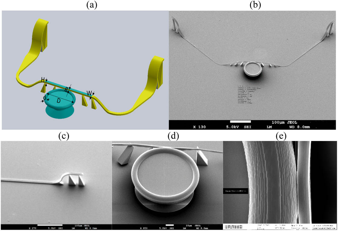
Figure 1.(a) Schematic and (b) SEM image of the fabricated integrated microtoroid-waveguide system; principal diameter
After fabrication, the optical property of the polymer microtoroid was characterized using a tunable laser covering the C- and L-bands and a fast photodetector. A fiber-based polarizer was used to select transverse electric (TE) light. In this work, polarization-maintaining lensed fibers were used to edge couple TE-polarized light into the system. The linear optical properties of the microtoroid-waveguide system are characterized by measuring the transmission spectra to extract the quality factor and group index of the resonator. The measured transmission spectrum is shown in Fig. 2(a). It reveals the characteristic dips of the WGM cavity. The free spectral range (FSR) at 1551 nm is measured to be 5.85 nm. The loaded quality factor of the microtoroid resonator is extracted from the transmission spectral Lorentzian fit, using equation , in which is the full width at half-maximum (FWHM). From Fig. 2(b), the loaded quality factor is extracted to be . The intrinsic quality factor is related to the loaded quality factor by
![]()
Figure 2.(a) Transmission spectrum of microtoroid resonator. Major diameter is 80 μm, minor diameter is 8 μm, and gap is 300 nm. (b) Lorentzian fitting of a single resonance at 1545.8 nm; (c) Lorentzian fitting of a single resonance at 1464.1 nm; (d) group index as a function of wavelength.
It is also noted that the maximum extinction ratio (ER) of is observed at 1464.1 nm, which is larger than the ER at 1545.8 nm (). Higher ER indicates the stronger coupling of light from the bus waveguide to the microcavity. The Lorentzian fit reveals a quality factor of 7850 at 1464.1 nm, as shown in Fig. 2(c), corresponding to the intrinsic quality factor of . This implies that the scattering losses are higher at 1464.1 nm compared to those at 1551 nm.
In the 3D printing process, the voxel size is limited to around 100 nm. This finite voxel size gives rise to some extent of roughness that may also be seen in the scanning electron microscopy (SEM) image of the microtoroid. From one fabrication run to the next, similar quality factors for the designed microtoroids are obtained. This is in line with the quality factor being limited by surface roughness induced by the finite voxel size rather than process variations. Based on the voxel size, we estimate a surface roughness on the order of 10 nm. We note further that lithographically defined and wet-etched silica microtoroid microresonators have high quality factors of and likely have much better roughness than our structures. To overcome the voxel limit in the surface roughness, postprocessing approaches potentially involving thermal or laser annealing could be investigated in the future, likely involving process precision so as not to compromise the small gaps between the coupling waveguide and microtoroid.
The group index can be extracted from the transmission spectra using the equation , where is the diameter of the microtoroid, and FSR is the free spectral range. The group index is calculated and plotted in Fig. 2(d). It is around 1.5 at the wavelength range of the measurement.
To verify our experimental results, we perform numerical simulations for the microtoroid resonators (, ). In our simulations, we use the 2.5D variational finite-difference time-domain (varFDTD) method, which offers comparable accuracy and versatility but requires significantly less simulation time and memory. Here, we employed the 2.5D varFDTD solver in MODE Solutions to calculate the transmission spectrum and the mode profile of our polymer microtoroid resonator. A gap of 300 nm and refractive index of 1.53 are used. Light (1545–1552 nm) enters the input port of the bus waveguide and perfectly matched layers (PMLs) are used as the boundary condition. The output power is collected from the output port of the bus waveguide. The transmission spectrum of the resonator [Fig. 3(a)], and the mode profiles of light on-resonance and off-resonance are recorded [Figs. 3(b) and 3(c)]. The FSR is calculated to be about 5.58 nm around the wavelength of 1551 nm, which is close to the measured FSR of 5.85 nm at 1551 nm. At resonance wavelengths, the energy is increased in the cavity, as shown in Fig. 3(b). At wavelengths far from resonance, most of the optical field is transmitted through the bus waveguide with negligible coupling into the microtoroid, as shown in Fig. 3(c).
![]()
Figure 3.(a) Simulated transmission spectrum of microtoroid resonator. The major and minor diameters are 80 μm and 8 μm, respectively, and the gap is 300 nm. (b) Simulated mode profile at 1545.78 nm (on-resonance) and (c) at 1549.3 nm (off-resonance).
To further investigate the performance of the integrated microtoroid-waveguide system, different gaps (200, 300, 400 nm) are fabricated to showcase the sensitivity of the microtoroid performance to the coupling waveguide’s position, as well as the precision in the fabricated waveguide placement availed by the 3D printing fabrication technique. The principal diameter and minor diameter are kept as 88 μm and 8 μm, respectively. The size of the coupling waveguide is 2 μm in width by 2 μm in height. Figures 4(a)–4(c) show SEM images of the coupling region between the microtoroid and coupling waveguide with gaps of 200, 300, and 400 nm, respectively. The transmission spectra of the microtoroid with various gaps are measured and shown in Fig. 4(d). It can be seen from Fig. 4(d) that a microtoroid with a gap of 300 nm (red line) offers the best resonator performance. The cavity resonances in this case have distinct, observable extinction. The transmission spectrum from the microtoroid-waveguide system with a 400 nm gap (yellow line) shows a spectrum that is nonrepresentative of a well-coupled resonator. The coupling gap is therefore too large. When the gap is reduced to 200 nm, however, we move to the regime of overcoupling. It is observed that in addition to the resonances with an FSR of , additional dips are present in the spectrum. These additional dips likely originate from the excitation of higher-order modes, which causes the resonator’s transmission spectrum to deteriorate. We note further that all fabricated microtoroid-waveguide parameters are identical, with the exception of the microtoroid-waveguide gap. We perform simulations of the microtoroid with varying gap widths of 200, 300, and 400 nm. The calculated spectra in Fig. 4(e) confirm that the coupling efficiency indeed changes with the gap. It is also clear that the 300 nm gap offers the highest extinction, whereas the 400 nm gap provides the lowest coupling efficiency among these three devices, in agreement with the measurements. A 100 nm nominal increase/decrease in the gap value causes significant changes in the transmission performance, confirming the sensitivity of the system’s performance to the placement of the coupling waveguide. Consequently, the ability for the 3D printed system to achieve precise placement of the coupling waveguide is an important function that can streamline ease of use and wide-scale deployment of microtoroid resonators. This demonstration further highlights the significance of the precise alignment when measuring microtoroid resonators, which is a big challenge when using nonintegrated optical fiber tapers for the measurement. With our designed integrated microtoroid-waveguide system, this problem is solved due to the precise and robust gap control during fabrication. Importantly, the entire microtoroid-waveguide system is 3D-printed in a single step, allowing the 3D nature of the system to be easily realized.
![]()
Figure 4.SEM images of coupling region between the microtoroid and coupling waveguide with a gap of (a) 200 nm; (b) 300 nm; and (c) 400 nm; (d) measured transmission spectra of the microtoroid-waveguide with gaps of 200 nm (blue line), 300 nm (red line), and 400 nm (yellow line); (e) simulated transmission spectra of microtoroid-waveguide with gaps of 200 nm (blue line), 300 nm (red line), and 400 nm (yellow line).
To further demonstrate the enhanced functionality of 3D printing for the realization of fully 3D photonic structures, 3D, nested double-spiral waveguides are fabricated and terminated with the air–bridge coupler on both input and output ends. Figures 5(a)–5(c) show scanning electron micrographs of the fabricated waveguides, the spiral region, and the input/output waveguide coupler. The transmission spectrum [Fig. 5(d)] reveals a flat transmission spectrum for ports of the nested spiral waveguide, with the 3 dB bandwidth spanning the entire measurement wavelength range of 1530 to 1610 nm; the transmission spectrum of the two waveguides is similar, as observed from the blue curve and the red curve in Fig. 5(d). The insertion loss of the nested double-spiral waveguide therefore ranges from 15 to 18 dB in this range.
![]()
Figure 5.(a) SEM image of nested double-spiral waveguide; scale bar is 100 μm; (b) magnified view of the spiral region; scale bar is 10 μm; (c) input and output waveguide coupler; scale bar is 10 μm; (d) transmission spectrum of the nested double-spiral waveguide.
Increasing the data density through the aforementioned nested spiral waveguide is availed by augmenting the spatial density of the waveguide. This feature is facilitated by the three- dimensionality in the 3D printing technique, allowing the vertical dimension to be leveraged for the waveguide design and positioning. Space-division multiplexing aims to elevate data capacities by increasing the density of guided wave structures in a given space [24]. The nested spiral waveguides provide a new paradigm which space-division multiplexing could be based on, a feature which no doubt relies on the truly 3D nature of the multiphoton lithography technique. Similar to spatial-division multiplexing, advanced modulation formats may also increase data capacities of light-wave communication systems. Advanced modulation formats such as PAM4 are being increasingly deployed in commercial products, both for short-haul applications (parallel single mode 4 lane (PSM4) [25]) and long-haul high-speed data movement (e.g., 100G Serial Lambda [26]). While NRZ remains the most common format for high-speed data transmission with direct detection, the augmented capacity availed by the increased number of bits in PAM4 modulation schemes has resulted in a gradual proliferation of PAM4 in replacing NRZ.
High-speed characterization was performed on the fabricated 3D-printed nested spiral waveguides. Pseudo-random bit sequence (PRBS31) was used with two different modulation formats: (i) 30 Gb/s NRZ, also known as “amplitude shift keying” (ASK) or PAM (two levels), and (ii) 28 GBaud per second PAM4. The experimental setup is shown in Fig. 6. With the help of its integrated laser function, an optical transmitter modulates the input electrical PRBS31 sequence from a bit error rate tester (BERT) into an optical signal of NRZ and PAM4 format. The wavelength is set to 1550 nm. The output is TE-polarized, amplified [erbium-doped fiber amplifier (EDFA1)], and filtered [bandpass filter (BPF1)] to remove noise introduced by EDFA1. The TE-polarized light is launched using a tapered fiber into the fabricated waveguide. The output was then amplified (EDFA2) and filtered (BPF2) before being fed into the photoreceiver for optical-to-electrical conversion. The converted signal was analyzed using a digital sampling oscilloscope (DSO) and its BER was characterized using the BERT receiver. The setup for PAM4 is the same as for NRZ, but using a BERT with PAM4 capability. The characterization is performed against a back-to-back (B2B) setup. The B2B setup is the same setup as in Fig. 6, but with the 3D printed waveguide replaced by an optical attenuator. The loss of the attenuator is equivalent to the insertion loss of the 3D printed waveguide.
![]()
Figure 6.High-speed testing setup using 30 Gb/s NRZ data and 28 Gb/s PAM4 data.
Figure 7(a) shows a plot of as a function of received power. It is compared against the B2B BER readings. Using a low received power of 3 dBm, we achieved a PAM4 BER of , which meets the forward error correction (FEC) threshold requirement. At the FEC threshold at , the power penalties for NRZ and PAM4 are 1.85 and 2.94 dB, respectively. Figures 7(b) and 7(c) show the eye diagrams for NRZ and PAM4, respectively. The high-speed characterization results show that our 3D printed waveguides are suitable for high-speed data transmission for both NRZ and the next-generation PAM4 signaling format.
![]()
Figure 7.(a) Plot of
Figure 7(d) shows the BER histogram characterized from the error detector of the BERT receiver. The BER histogram is an alternative method to an eye diagram for analyzing the bit-level distribution of a PAM4 signal graphically [27]. It is observed that the four-bit levels are distinct, corroborating the open PAM4 eye experimentally observed in Fig. 7(c) and confirming the waveguide’s ability satisfying the minimum FEC BER limit for error correction. We note that we have investigated space-division multiplexing from the standpoint that the amount of data can be increased by adding another waveguide that is spatially parallel to the first spiral waveguide. In the future, multiplexing based on wavelength and polarization can be investigated to further augment the aggregate data rates available in the waveguide.
4. CONCLUSION
In this paper, a monolithically integrated polymer microtoroid resonator-waveguide system was proposed and fabricated using 3D printing based on multiphoton lithography. Importantly, we introduce a technique which circumvents the need for heterogeneous, fiber-based coupling of light to a microtoroid resonator, a process that requires high alignment precision and is cumbersome to execute. By leveraging the 3D design freedom availed in the 3D printing technique, the full 3D morphology of the microtoroid resonator and a suspended coupling waveguide precisely aligned with a 300 nm gap and matching the vertical height of the microtoroid is demonstrated. We further experimentally verify the sensitivity of the microtoroid output spectrum to the magnitude of the coupling gap, as well as the ability to precisely position the coupling waveguide. In addition, we introduce nested double-spiral waveguides, which can potentially be used as a vessel for space-division multiplexed systems. The spiral waveguides are further demonstrated for 30 Gb/s NRZ and 28 Gb/s PAM4 data transmission, allowing two dimensions of augmented data transmission from space-division multiplexing and advanced modulation formats. The results showcase the design degrees of freedom that are made available by 3D-printed, multiphoton lithographically fabricated photonic devices.
References
[1] Y. P. Gao, C. Cao, T. J. Wang, Y. Zhang, C. Wang. Cavity-mediated coupling of phonons and magnons. Phys. Rev. A, 96, 023826(2017).
[2] X. F. Liu, T. J. Wang, Y. P. Gao, C. Cao, C. Wang. Chiral microresonator assisted by Rydberg-atom ensembles. Phys. Rev. A, 98, 033824(2018).
[3] Z. Shen, Y. L. Zhang, Y. Chen, C. L. Zou, Y. F. Xiao, X. B. Zou, F. W. Sun, G. C. Guo, C. H. Dong. Experimental realization of optomechanically induced nonreciprocity. Nat. Photonics, 10, 657-661(2016).
[4] L. Tian. Optoelectromechanical transducer: reversible conversion between microwave and optical photons. Ann. Phys., 527, 1-14(2015).
[5] R. Osellame. New effective technique to produce waveguides in lithium niobate on insulator (LNOI). Quantum Eng., 1, e11(2019).
[6] M. Wang, R. Wu, J. Lin, J. Zhang, Z. Fang, Z. Chai, Y. Cheng. Chemo-mechanical polish lithography: a pathway to low loss large-scale photonic integration on lithium niobate on insulator. Quantum Eng., 1, e9(2019).
[7] F. Bo, J. Wang, J. Cui, S. K. Ozdemir, Y. Kong, G. Zhang, J. Xu, L. Yang. Lithium niobate–silica hybrid whispering-gallery-mode resonators. Adv. Mater., 27, 8075-8081(2015).
[8] Q. T. Cao, H. Wang, C. H. Dong, H. Jing, R. S. Liu, X. Chen, L. Ge, Q. Gong, Y.-F. Xiao. Experimental demonstration of spontaneous chirality in a nonlinear microresonator. Phys. Rev. Lett., 118, 033901(2017).
[9] X. Yang, Ş. K. Özdemir, B. Peng, H. Yilmaz, F. C. Lei, G. L. Long, L. Yang. Raman gain induced mode evolution and on-demand coupling control in whispering gallery-mode microcavities. Opt. Express, 23, 29573-29583(2015).
[10] S. H. Huang, S. Sheth, E. Jain, X. Jiang, S. P. Zustiak, L. Yang. Whispering gallery mode resonator sensor for in situ measurements of hydrogel gelation. Opt. Express, 26, 51-62(2018).
[11] F. Vollmer, S. Arnold. Whispering-gallery-mode biosensing: label-free detection down to single molecules. Nat. Methods, 5, 591-596(2008).
[12] S. Yu. Manipulating optical vortices using photonic integration. AAPPS Bull., 25, 19-24(2015).
[13] H. Fan, X. Gu, D. Zhou, H. Fan, L. Fan, C. Xia. Confined whispering-gallery mode in silica double-toroid microcavities for optical sensing and trapping. Opt. Commun., 434, 97-103(2019).
[14] Y. Wang, S. Li, S. Kiravittaya, X. Wu, K. Wu, X. Li, Y. Mei. Mode-splitting based optofluidic sensing at exceptional points in tubular microcavities. Opt. Commun., 446, 128-133(2019).
[15] G. Q. Qin, H. Yang, X. Mao, J. W. Wen, M. Wang, D. Ruan, G. L. Long. Manipulation of optomechanically induced transparency and absorption by indirectly coupling to an auxiliary cavity mode. Opt. Express, 28, 580-592(2020).
[16] M. Wang, Y. Z. Wang, X. S. Xu, Y. Q. Hu, G. L. Long. Characterization of microresonator-geometry-deformation for cavity optomechanics. Opt. Express, 27, 63-73(2019).
[17] T. Wang, Y. Q. Hu, C. G. Du, G. L. Long. Multiple EIT and EIA in optical microresonators. Opt. Express, 27, 7344-7353(2019).
[18] F. C. Lei, M. Gao, C. Du, Q. L. Jing, G. L. Long. Three-pathway electromagnetically induced transparency in coupled-cavity optomechanical system. Opt. Express, 23, 11508-11517(2015).
[19] D. E. Liu. Sensing Kondo correlations in a suspended carbon nanotube mechanical resonator with spin-orbit coupling. Quantum Eng., 1, e10(2019).
[20] J. Richter, M. P. Nezhad, J. Witzens. High-
[21] H. Gao, G. F. R. Chen, P. Xing, J. W. Choi, H. Y. Low, D. T. H. Tan. High-resolution 3D printed photonic waveguide devices. Adv. Opt. Mater., 8, 2000613(2020).
[22] A. Nesic, M. Blaicher, T. Hoose, A. Hofmann, M. Lauermann, Y. Kutuvantavida, M. Nöllenburg, S. Randel, W. Freude, C. Koos. Photonic-integrated circuits with non-planar topologies realized by 3D-printed waveguide overpasses. Opt. Express, 27, 17402-17425(2019).
[23] N. Lindenmann, G. Balthasar, D. Hillerkuss, R. Schmogrow, M. Jordan, J. Leuthold, W. Freude, C. Koos. Photonic wire bonding: a novel concept for chip-scale interconnects. Opt. Express, 20, 17667-17677(2012).
[24] D. Richardson, J. Fini, L. Nelson. Space-division multiplexing in optical fibres. Nat. Photonics, 7, 354-362(2013).
[25] . 100G PSM4 specification(2020).
[26] https://100glambda.com/. https://100glambda.com/
[27] L. Ding, W.-D. Zhong, C. Lu, Y. Wang. New bit-error-rate monitoring technique based on histograms and curve fitting. Opt. Express, 12, 2507-2511(2004).

Set citation alerts for the article
Please enter your email address
© Copyright 2018-2021 | Chinese Laser Press. All Rights Reserved 沪ICP备15018463号-20