• Chinese Optics Letters
  • Vol. 19, Issue 3, 031901 (2021)
Yan Guan1, Fang Wang2, Ying Yang2, Deen Wang2, Xin Zhang2, Qiang Yuan2, Dongxia Hu2、3, Xuewei Deng2、3、*, Huaijin Ren4, Yuanlin Zheng1, and Xianfeng Chen1、5、**
Author Affiliations
  • 1State Key Laboratory of Advanced Optical Communication Systems and Networks, School of Physics and Astronomy, Shanghai Jiao Tong University, Shanghai 200240, China
  • 2Laser Fusion Research Center, China Academy of Engineering Physics, Mianyang 621900, China
  • 3IFSA Collaborative Innovation Center, Shanghai Jiao Tong University, Shanghai 200240, China
  • 4Institute of Applied Electronics, China Academy of Engineering Physics, Mianyang 621900, China
  • 5Collaborative Innovation Center of Light Manipulation and Applications, Shangdong Normal University, Jinan 250358, China
  • show less
    DOI: 10.3788/COL202119.031901 Cite this Article Set citation alerts
    Yan Guan, Fang Wang, Ying Yang, Deen Wang, Xin Zhang, Qiang Yuan, Dongxia Hu, Xuewei Deng, Huaijin Ren, Yuanlin Zheng, Xianfeng Chen. Variation in linear susceptibility tensor at crystal surface probed by linear Cherenkov radiation[J]. Chinese Optics Letters, 2021, 19(3): 031901 Copy Citation Text show less
    Phase-matching scheme of CSHG.
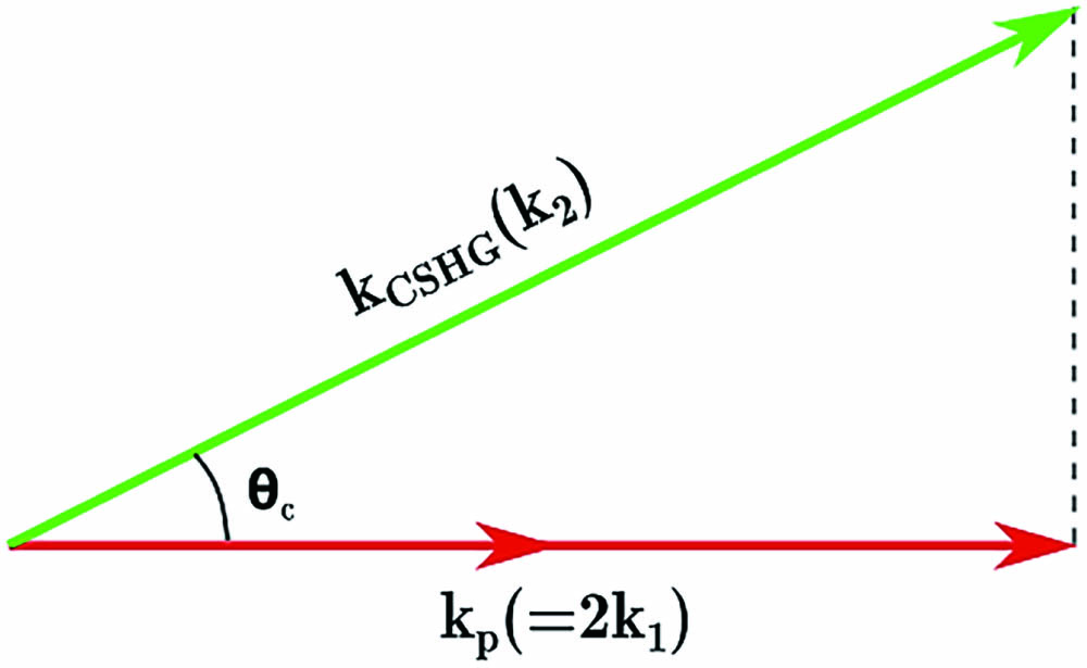
    Fig. 1. Phase-matching scheme of CSHG.
    (a) Phase-matching scheme of CSHG for oblique incidence. (b) Phase-matching scheme of LCR for oblique incidence.
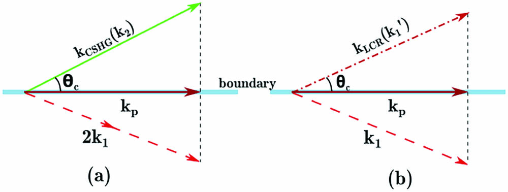
    Fig. 2. (a) Phase-matching scheme of CSHG for oblique incidence. (b) Phase-matching scheme of LCR for oblique incidence.
    Light path scheme of LCR processes at the KDP surface.
    Fig. 3. Light path scheme of LCR processes at the KDP surface.
    Schematic of the main experiment set-up.
    Fig. 4. Schematic of the main experiment set-up.
    Schematic of KDP placement on the rotation stage.
    Fig. 5. Schematic of KDP placement on the rotation stage.
    Photos of screen (right) and phase-matching analysis (left) of four serial experiments. All of these photos are under the condition that incident beam contains both o- and e- polarization states. (a) Using 1053 nm incident beam; optical axis of KDP is like Fig. 5(a). (b) Using 1053 nm incident beam; optical axis of KDP is like Fig. 5(b). (c) Using 526.5 nm incident beam; optical axis of KDP is like Fig. 5(a). (d) Using 526.5 nm incident beam; optical axis of KDP is like Fig. 5(b).
    Fig. 6. Photos of screen (right) and phase-matching analysis (left) of four serial experiments. All of these photos are under the condition that incident beam contains both o- and e- polarization states. (a) Using 1053 nm incident beam; optical axis of KDP is like Fig. 5(a). (b) Using 1053 nm incident beam; optical axis of KDP is like Fig. 5(b). (c) Using 526.5 nm incident beam; optical axis of KDP is like Fig. 5(a). (d) Using 526.5 nm incident beam; optical axis of KDP is like Fig. 5(b).
    Theoretical predictions and measured results in the experiment on the relationship of external LCR emitting angles θ1 and θ2.
    Fig. 7. Theoretical predictions and measured results in the experiment on the relationship of external LCR emitting angles θ1 and θ2.
    Optical Axis OrientationConversion TypeIncident Electric Field ComponentsLCR Electric Field ComponentsNew Nonzero Elements in χ(1) (underlined)Remarks
    Figure 5(a)o to eEx & EyEx, Ey, & Ez(χ11000χ110χ31χ32χ33)χ31, χ32 cannot be zero at the same time
    e to oEx, Ey, & EzEx & Ey(χ11000χ11000χ33)No new nonzero element is necessary simply considering the polarization state
    Figure 5(b)o to eEx & EyEz(χ11000χ110χ31χ32χ33)χ31, χ32 cannot be zero at the same time
    e to oEzEx or Ey or Ex & Ey(χ110χ130χ11χ2300χ33)χ13, χ23 cannot be zero at the same time
    Table 1. The Relationship of Polarization State and Nonzero Elements
    Yan Guan, Fang Wang, Ying Yang, Deen Wang, Xin Zhang, Qiang Yuan, Dongxia Hu, Xuewei Deng, Huaijin Ren, Yuanlin Zheng, Xianfeng Chen. Variation in linear susceptibility tensor at crystal surface probed by linear Cherenkov radiation[J]. Chinese Optics Letters, 2021, 19(3): 031901
    Download Citation