1Department of Physics, Shanghai Key Laboratory of Materials Protection and Advanced Materials in Electric Power, Shanghai University of Electric Power, Shanghai 200090, China
2State Key Laboratory of Advanced Optical Communication Systems and Networks, School of Physics and Astronomy, Shanghai Jiao Tong University, Shanghai 200240, China
3Collaborative Innovation Center of Light Manipulation and Applications, Shandong Normal University, Jinan 250358, China
Recently, all-inorganic halide perovskites have received enormous attention because of their excellent optoelectronic properties. Among them, the power conversion efficiency (PCE) of all-inorganic halide perovskite solar cells has made rapid progress in the last few years. However, understanding the intrinsic physical nature of halide perovskites, especially the dynamic process of photo-generated carriers, is a key for improving the PCE. In this review, we introduced and summarized the photoluminescence (PL) technique used to explore the carrier dynamic process in all-inorganic halide perovskites. Several physical models were proposed to investigate the dynamic parameters, i.e., recombination lifetime and diffusion length, by analyzing the steady-state PL as well as the time-resolved PL spectra. We also discussed the distinction of PL spectral behavior between bulk halide perovskite samples and those grown with transport layers due to the participation of different dominant dynamic paths. Finally, we briefly described some other optical techniques reported to study the relevant physical properties of all-inorganic halide perovskites.
1. INTRODUCTION
Halide perovskite materials have developed rapidly due to their exceptional optoelectronic properties and low-cost fabrication processes. The initial studies were focused on organic–inorganic hybrid perovskites; however, up to now, they still go through some compositional and structural degradation mechanisms, leading to thermal and chemical instabilities [1–7]. To realize future commercialization, we need to pursue low cost, high efficiency, and high stability, which is inseparable from the excellent performance of the material. Fortunately, all-inorganic halide perovskites display both high stability and remarkable optoelectronic properties, with long carrier recombination lifetime [8–11], long diffusion length [12,13], and strong optical absorption [14], which render them as an intriguing and promising semiconductor for a broad range of applications including perovskite solar cells (PSCs), photodetectors, light-emitting diodes (LEDs), and lasing [15–25]. These properties have led to rapid increases in the efficiency of PSCs and LEDs over a short period of time [26].
The study of carrier dynamics in all-inorganic halide perovskites, i.e., recombination and transport, is necessary to better understand their photoelectronic applications. Therefore, the relevant physical parameters are usually measured and discussed in the newly grown halide perovskite samples by different techniques, among which photoluminescence (PL) is widely employed. As we know, the dynamic process of carriers in semiconductor materials is rather complex, especially in the non-equilibrium state. The photo-generated carriers will go through several paths such as recombination and diffusion. By using steady-state PL (SSPL) and time-resolved PL (TRPL) techniques, researchers have established theoretical models, which can be utilized to deeply analyze the dynamic process inside the materials. Although the PL technique has been widely used to explore the dynamic physics of all-inorganic halide perovskites recently, there is no systematic report on it up to now. Moreover, we should be aware that the PL characteristics as well as the corresponding conclusions may be completely opposite for the samples with or without carrier transport layers (TLs). This is what often confused people.
In this work, we reviewed the investigation of the carrier dynamic process of all-inorganic halide perovskite materials using the PL technique. This article is divided into four parts: in the first section, we introduced the overall existed carrier dynamics in halide perovskite materials, including recombination and transport; in the second section, we presented the application of SSPL and TRPL to the study of the carrier relaxation process in all-inorganic halide perovskites; in the third part, carrier dynamics in all-inorganic halide perovskites with TLs through a PL experiment were discussed in detail, where we focused on the efficiency of photo-induced carrier transfer into the electron (or hole) TL, and the way to obtain diffusion coefficient and length was also demonstrated; finally, we briefly discussed the limitation of PL spectra and introduced other techniques employed to study carrier lifetime. Throughout the whole article, in addition to reviewing the application of PL spectra in the analysis of carrier dynamics, the corresponding data and conclusions of all-inorganic halide perovskite materials reported in recent years were also summarized and discussed.
Sign up for Photonics Research TOC. Get the latest issue of Photonics Research delivered right to you!Sign up now
2. CARRIER DYNAMIC PROCESS IN SEMICONDUCTORS
Typically, in most semiconductor materials, carrier dynamics mainly refer to two processes: recombination and transport. As for recombination, there are three different routes after carrier excitation by absorption: radiative recombination, non-radiative Shockley−Read−Hall (SRH) recombination, and Auger recombination. They are also related to the mono-molecular, bi-molecular, and tri-molecular processes of optical relaxation, respectively. In the radiative recombination event, an electron−hole pair is annihilated to emit the photon and thus generate the PL signal. The SRH recombination is related to the presence of defects. The excited carriers are captured by the defect sites, and then they gradually relax towards the ground state (GS) by the emission of phonons. The process of Auger recombination involves non-radiative transfer of the excess energy due to electron−hole recombination to a third charge carrier (electron or hole), which is ejected from its original state.
3. CARRIER RECOMBINATION DECAY IN ALL-INORGANIC HALIDE PEROVSKITES BY PL SPECTRA
A. SSPL
PL spectroscopy is a keystone characterization technique to explore properties of the carrier relaxation process [40]. Most of the grown all-inorganic halide perovskites employed this special method to characterize the properties of the materials. For the SSPL spectrum, the position of the peak refers to the band gap energy, which corresponds to the absorption edge. Furthermore, the full width at half-maximum (FWHM) of the peak as well as the band tail can qualitatively reflect the homogeneity of the material. Besides that, the information of the carrier recombination process can also be extracted by the SSPL spectrum, and this is the focus of our discussion below.
The mechanism of recombination can be estimated by the power dependence of the steady-state integrated PL intensity and the excitation density as [41]. It reveals a linear relationship in a log−log plot, and the fitted slope of this line is , by which the recombination mechanism can be determined qualitatively. There is a long-standing controversy whether free carriers or excitons are generated in perovskites upon photoexcitation. Thus, the value is helpful to study the competition between exciton and free carrier: for free carrier recombination, for recombination of excitons, and for free-to-bound recombination [42]. Another viewpoint is proposed by Saba et al. according to a trap-assisted recombination model, that should equal 1.5 when the majority of TS were unoccupied, and it gradually decreased to 1 when the trap density decreased [43]. Later, Chirvony et al. pointed out that if the PL intensity dependence with was observed, then it implied that the PL quantum yield (PLQY) remained constant [34]. Recently, a more intuitive argument was declared [40]. As it indicated, the two basic patterns are expected: mono-molecular, i.e., linear, and bi-molecular, that in some conditions translates into quadratic dependence. As it argued, in some cases, the intermediate case ( between 1 and 2), i.e., mixture of these two, is expected.
Figure 2.(a) Integrated PL intensity linearly increasing with excitation power in NCs. Reprinted with permission [27]. (b) Fitting results of excitation density dependent PL spectra of the pristine and TOPO-treated perovskite films. Reprinted with permission [46]. (c) Power-dependent emission spectra indicating lasing of nanowires. Inset: a two-dimensional pseudo-color plot of emission spectra at different pump fluences. (d) The power dependence of the integrated emission intensity and the FWHM of the dominant emitted lasing peak. Reprinted with permission [47].
Power-dependent PL intensity was also effective for studying lasing properties, which is a very important application of all-inorganic perovskites. Among them, the nanowires/nanoribbons are one of the most competitive materials [25,47,48]. For example, Fig. 2(c) exhibits the power-dependent emission spectra of an individual nanowire, and Fig. 2(d) shows the plot of the intensity and the FWHM of emission peaks versus the excitation power [47]. A typical “S” curve revealed in Fig. 2(d) indicates the transition processes from spontaneous emission to the full lasing status. Meanwhile, at the lasing threshold of μ, a sharp decrease in the FWHM is observed. By fitting the lasing rate equation, the spontaneous emission factor can be obtained, which has a certain reference guideline for lasing investigation.
B. TRPL Techniques
Figure 3.Simulated TRPL curves. Solid lines were calculated by single exponential function using different lifetimes of 1 ns (red), 2 ns (blue), and 10 ns (green). Dashed curves were calculated using the double exponential formula by fixing two lifetimes of and , with a change of their weighted amplitude .
Most of the reported lifetimes of all-inorganic halide perovskite materials that satisfy the single exponential relationship are in the range of 1–30 ns [49–54], as listed in Table 1. Li et al. investigated the effects of phase transition as well as doping (Cl) on the carrier lifetime of thin films [50]. PL decay for the pure orthorhombic films exhibited a time constant of 6.7 ns, while of cubic film was 12.3 ns. Therefore, the phase transition of orthorhombic-to-cubic for induced a significant increase in exciton lifetime. While for Cl-doped cubic , further increased to 14.3 ns, exhibiting a longer carrier lifetime. Ren et al. introduced the polyethylene glycol (PEG) into the precursor solution during the growth of film through a one-step spin-coating process [53]. They declared that the PEG-aided perovskite thin film would have higher homogeneity since it did not induce any excessive non-radiative recombination. This deduction can be confirmed by the TRPL experiment, where the film with PEG showed longer PL lifetime (32.1 ns) than that without the PEG additive (11.8 ns), indicating the beneficial influence of PEG on the thin film quality [68,69].
Perovskite Material
Year
Model
τave (ns)
τ1 (ns)
A1
τ2 (ns)
A2
τ3 (ns)
A3
Reference
CsPbBr3 orthorhombic
2017
Single
6.7
[50]
CsPbBr3 cubic
12.3
CsPbI2Br film
2018
Single
8.6
[51]
CsPbBr3−xIx QDs
2018
Single
3.57–10
[52]
CsPbI2Br/Spiro-OMeTAD
2019
Single
4.6
[49]
CsPbI2Br/(CsPbI2Br)1−x(CsPbI3)x/Spiro-OMeTAD
3.2
CsPbBr3 with PEG
2020
Single
32.1
[53]
CsPbBr3 without PEG
11.8
CsPbI3
2020
Single
0.553
[54]
PEAI-CsPbI3
15.358
CsPbI2Br (GTA)
2019
Double
4.3
1.964
0.12
4.478
0.88
[55]
CsPbI2Br (GTA-AST-Tol)
6.9
1.950
0.056
7.032
0.94
CsPbI2Br (GTA-AST-IPA)
14.1
4.806
0.12
14.516
0.88
CsPbI2Br
2019
Double
11.27
6.57
0.372
14.31
0.617
[56]
CsPbI2Br
2017
Double
14
4.6
0.28
18
0.72
[57]
Cs0.025K0.075PbI2Br
11
4
0.3
14
0.7
CsPbI2Br
2017
Double
2.2
11.1
[58]
CsPb0.98Sr0.02I2Br
2.1
17.1
CsPb0.95Ca0.05I3
2018
Double
6.6
2.3
8.1
[59]
CsPbI2Br
2019
Double
0.453
0.453
0.438
[60]
CsPbI2Br(0.5%Nb)
2.287
2.125
3.875
CsPbI2Br
2019
Double
2.01
2.67
0.64
1.08
0.36
[61]
CsPbI2Br(0.5%BaI2)
16.0
11.8
0.59
22.1
0.41
CsPbI2Br
2020
Double
20.57
12.95
0.25
23.0
0.75
[62]
CsPb0.98La0.02I2Br
48.73
10.01
0.0652
851.43
0.935
CsPbBr3 cubic
2018
Double
35.67
56.03
0.49
16.14
0.51
[63]
CsPbBrxI1−xNCs
2019
Double
6.07
2.93
0.76
16.05
0.24
[64]
CsPbBr3
2020
Double
13.65
3.38
0.92
27.33
0.08
[65]
CsPbBr3 with IPA treatment
43.21
9.97
0.77
61.39
0.23
CsPbI2Br NCs
2018
Triple
6.91
2.09
0.079
5.19
0.604
11.41
0.317
[66]
CsPbBr3 NCs
2018
Triple
0.9
0.3
0.56
0.8
0.43
4.5
0.01
[29]
Cs2AgBiBr6NCs
2018
Triple
0.05
1
100
[28]
CsPbX3 NCs
2019
Triple
1.34–7.9
[67]
CsPbBr3 NCs
2019
Triple
0.294
1.261
6.054
[27]
Table 1. Summary of the Reported Lifetime by Single Exponential Fitting, Average Lifetime, Its Individual Lifetime and Amplitude by Double and Triple Exponential Fitting in All-Inorganic Halide Perovskites
Figure 4.(a) perovskite films with and without pre-coating of PVP on the substrate and (b) pristine, TOPO-treated, and TOPO/PMMA-treated perovskite films. Reprinted with permission [46].
When and no longer satisfy the single exponential relationship, it is necessary to use double or triple exponential fitting. For the double exponential relation, the form of is usually employed [60–77], where and represent the two fitted lifetime components of the decay curve, and , are their weighted amplitudes. In Fig. 3, we also plotted the calculated PL decay curves using the above double exponential formula. Three different combinations of and were simulated (red short dotted curve: and , blue short dotted curve: and , green short dotted curve: and ), while the values of and were fixed to be 2 and 10 ns, respectively. It can be seen that the three curves were all between the two single exponential curves [ (blue solid curve) and (green solid curve)]. With the decrease of the value, the simulated double exponential curve gradually moved away from and approached the single exponential curve. Therefore, we can not only extract the lifetimes of two relaxation processes, but also obtain the corresponding weight by fitting the experimental TRPL curve, which may be helpful for analyzing the different carrier dynamic processes in combination with the structural characteristics of halide perovskite materials.
Figure 5.(a) TRPL plots of the films fabricated on a glass substrate, treated by the GTA, GTA-ATS-Tol, and GTA-ATS-IPA processes. Inset: SSPL spectra of the corresponding films. Reprinted with permission [55]. (b) PL and (c) TRPL spectra of 0 and 0.5% Nb-doped films. Reprinted with permission [60]. (d) TRPL decay curves obtained for NCs with halogen ions varying from Cl to I. Reprinted with permission [67]. (e) TRPL decay profile and (f) temperature-dependent average lifetime of NCs. Reprinted with permission [27].
More research teams have studied the carrier lifetime of doping other elements into perovskites and found that the lifetimes increased to a certain extent due to the incorporation [60–62]. The identification of the two lifetime components extracted by fitting TRPL curves using a double exponential function in the reported materials was similar; that is, the shorter lifetime corresponded to the non-radiative recombination caused by defects or surface states, and the longer lifetime referred to the intrinsic radiative recombination.
Guo et al. studied the effect of niobium (Nb) doping into film on the electron extraction and transport process [60]. The SSPL intensity sharply increased after 0.5% Nb incorporation, as shown in Fig. 5(b), which indicates fewer traps and defects [78]. Thus, 0.5% Nb doping can significantly reduce the traps and defects in the perovskite film, meaning a better film quality and promising better performance [79,80]. The fitted average lifetime of the carrier dynamic process [Fig. 5(c)] was also increased from 0.453 ns (reference film) to 2.287 ns (0.5% Nb-doped film). Therefore, Nb doping may suppress the recombination process in the perovskite film, which was consistent with the performances of the PSC devices [81,82]. Another barium () alkaline earth metal cation was also proposed to be doped into perovskite [61]. Compared with the pristine , the TRPL decay profile exhibited increased PL lifetime upon incorporation. Moreover, both the surface and bulk recombination lifetimes were substantially prolonged from 2.01 to 16 ns, suggesting suppression of non-radiative recombination pathways in perovskite thin films, which were also consistent with the improved photovoltaic performance.
Another common type of doping is the substitution of Pb atoms in to form five element perovskite materials. Lau et al. incorporated the less toxic strontium () at a low concentration that partially substituted Pb in with changing from 0 to 0.05 [58]. The fitted defect trapping lifetime (fast component) of all the films was relatively the same, with a value of 2 ns. However, as the Sr content increased from 1% to 2%, the effective recombination lifetime (slow component) increased from 11.1 to 17.1 ns, suggesting a better effective recombination lifetime. This suggests better surface passivation provided by the Sr enriched surface. However, as the Sr content increased further, the excess doping in the perovskite film enhanced electron−hole recombination. Similar halide perovskite compounds formed by lanthanum () substitution doping were , reported by Chen et al. recently [62]. Through fitting the PL decay curves, the average carrier lifetimes for and were calculated to be 20.57 and 48.73 ns, respectively. The carrier lifetime at 2% doping was twice that of the pristine thin film, indicating that the film defects were greatly passivated after doping, which reduced the non-radiative recombination. However, similar to the case of Sr doping as discussed above, by further increasing the doping concentration to 3%, the carrier lifetime was sharply reduced, which may be due to the introduction of defects by excess ions.
For the more complex relaxation processes, it is necessary to use the three exponential relationship to better fit the TRPL curve: , where , , and represent the three fitted lifetime components, and , , and are their corresponding weighted amplitudes. The average lifetime is calculated by the formula or . Table 1 also lists the reported samples that used three exponential fitting. It is interesting to find that most of these perovskites were nanostructured materials [27–29,67,83]. Chen et al. studied the TRPL decay curves [Fig. 5(d)] of (, Br, I, Cl/Br, and Br/I) NCs by three exponential components, containing types of defect emissions in doping and surface defect emission [83]. The obtained average lifetimes were in the range from 1.34 ns () to 7.9 ns (). It was argued that the average lifetime was related to the size of the NCs. The larger size of NCs decreased the probability of carriers approaching the surface, leading to the lower non-radiative recombination rate and higher PLQY (about 70%) due to the enhanced radiation process.
Shi et al. investigated the TRPL decay curves of NCs deeply [27]. The curve could be globally fitted smoothly with a short time (), an intermediate time (), and a long time () with different amplitudes, as shown in Fig. 5(e). The short lifetime of 0.294 ns corresponded to the direct recombination of excitons in the material, which contributed to the PL fast decay in colloidal NCs, while the intermediate (long) time constant corresponded to the photo-excited electrons (holes) path along trapping–detrapping recombination with holes (electrons), contributing to the PL slow decay. The above deduction was further confirmed by the thermal effect, which could increase the TS and reduce the detrapping effect, changing the occupied percentage of indirect and direct recombination for excitons. As plotted in Fig. 5(f), the exciton mainly underwent indirect recombination at low temperature, balanced at the temperature of 130–150 K, and direct recombination at high temperature.
We noticed that either the photo-generated carriers or excitons have been mentioned by different groups in all-inorganic halide perovskites. However, the coexistence of free carriers and excitons as well as typical excitonic effects such as exciton resonance [84], exciton localization [85], and exciton polaritons [86] may be the potential situation. In the case of the coexistence of carriers and excitons, the exponential relationship may not be available, and some other theories have been proposed. For example, a stretched exponential formula was employed to calculate the lifetime of orthorhombic , and the fitting values of and were 50 ns and 0.66 [87]. Another reported fitting model is the thermalized stretching exponential line [88–90]:
The above model is regarded as evidence of the exciton localization, in which the parameter is related to the dimensionality of the localizing canters. The former exponential term in Eq. (1) represents the relaxation of free or extended states towards localized states, whereas the latter stretched exponential term accounts for the communication between the localized states. , and , are the corresponding weight fractions and decay times for free and localized excitons. Dey et al. used this theory to study the dynamic process of NC film, and the extracted values of and at 300 K were 3.64 and 8.16 ns, respectively [91]. When the temperature decreased from 300 to 10 K, the free exciton lifetime decreased first and then increased, while the local exciton lifetime monotonically decreased. Further, the value of is higher () at 300 K and then reduced to at 10 K, which reflected the distribution of traps and the corresponding trapped exciton release rates.
Changing the incident excitation energy can not only affect the SSPL as discussed above, but it also affects the TRPL spectrum, especially the PL intensity just after photoexcitation. However, the former focuses on the discussion of the recombination mechanism, while the latter is generally a good indicator of the nature of the radiative recombination processes [92]. In short, the initial PL intensity () is mainly linear with the photoexcitation density for the exciton recombination and proportional to for free carrier recombination, respectively [93–95].
Figure 6.(a) PL intensity just after photoexcitation as a function of carrier density of double halide perovskite film. Reprinted with permission [71]. (b) Initial PL intensity after laser excitation as a function of injected carrier density with the quadratic dependence at lower injected carrier density in the range of (solid red line) of halide perovskite film. Reprinted with permission [87]. (c) Lifetime and versus pump fluence in nanowires. Reprinted with permission [96].
Fu et al. studied the initial PL intensity just after excitation as a function of carrier density of the perovskite film [87]. As shown in Fig. 6(b), PL intensity increased quadratically with carrier density from to and then approached saturation at higher carrier densities. It is considered that at low density, this quadratic dependence revealed that the photo-excited carriers were mainly free carriers, and the emission was dominated by free carrier bi-molecular recombination. As the density increased (), a higher-order recombination channel (i.e., Auger recombination) may appear. A similar phenomenon was also observed in the relationship between PLQY and incident carrier density of the concerned samples.
To confirm the origin of the recombination process in nanowires, Li et al. extracted out the power-dependent PL lifetime and initial intensity , as shown in Fig. 6(c) [96]. By increasing the incident pump fluence, the PL lifetime decreases, while the is nearly linear with the excitation density. These results suggest that free carrier recombination is the main source of emission under the current excitation condition. The author also noted that the binding energy () is higher than the thermal energy at room temperature; however, they speculated that the high-power laser excitation may induce an increase to the local temperature and lead to exciton dissociation.
C. Temperature Effect on PL
The temperature dependency of PL spectra gives useful information about the physical properties in all-inorganic halide perovskites such as exciton binding energy, longitudinal optical (LO) phonon energy, exciton−phonon coupling strength, and the density of defects. Among them, the exciton binding energy and the exciton–phonon coupling strength are key parameters to clarify the nature of photo-generated charges, that is, free carriers or excitons. This will help interpret the counterintuitive fact that perovskites can act both as extraordinary photovoltaic materials and superior gain media for lasing. In general, photovoltaic materials require efficient separation of photocarriers, while lasing materials require high recombination rates [97,98].
Figure 7.(a) Temperature-dependent PL spectra for nanowires within the range of 80–295 K. The emission peak shows an evident blue shift (black arrow) and broadening with increasing temperature. (b) Temperature dependence of the FWHM extracted out from (a). Reprinted with permission [96]. (c) FWHM as a function of temperature of sphere. Reprinted with permission [100]. (d) Temperature-dependent PL decay curves of colloidal QDs with the temperature ranging from 80 to 380 K. (e) Average PL lifetimes of NCs for NC493, NC512, and NC516 samples at various temperatures. Reprinted with permission [104].
The extracted parameters of the studied nanowires are also listed in Fig. 7(b), where the inhomogeneous line width is 14.13 meV, arising from the scatterings with disorder and imperfections, and the exciton–LO phonon coupling coefficient is about 88.45 meV. Moreover, the authors mentioned that the obtained data are smaller than the previous reported values for nanowires with different widths [47], which may be caused by the effect of lattice distortion.
Similar investigations were carried out in microsphere cavities for lasing applications [100]. It is found that phonons of different energies are dominant at different temperature regions, as shown in Fig. 7(c) with the fitted parameters correspondingly. Besides, the exciton–phonon coupling strength in region II is much stronger than that in region I. Thus, the authors conjectured that two different phonon modes participated in the exciton–phonon scattering, and the LO energy of 15.3 meV is more significant.
The exciton binding energy can be simulated by fitting the temperature dependency of the PL intensity of the SSPL spectra using an Arrhenius equation [101,102]: where is the intensity at 0 K, is the exciton binding energy, which is also related to the thermal activation energy if no other exciton decay channel exists [103,104], and is the Boltzmann constant.
For inorganic perovskites, the temperature effect in nanomaterials was relatively widely studied [91,103–110], and most of the applied temperature range was 80–300 K. However, a very low temperature (below 10 K) [91,105,106] or higher temperature (up to 380 K) [104,107,109] was also investigated. The calculated exciton binding energies from the above research groups are listed in Table 2. It is found that most of the energy is larger than thermal energy of about 25.9 meV at room temperature (300 K), which means that the excitons in nanoscale materials should be very stable at room temperature.
Perovskite Material
Year
Exciton Binding Energy (meV)
Reference
CsPbBr3 15 nm thick nanowires
2018
93
[111]
CsPbBr3 250 nm thick nanowires
65
CsPbBr3 QDs with 5.5 nm size
2017
50
[106]
CsPbBr3 QDs with 7.3 nm size
48
CsPbBr3 QDs with 10.1 nm size
34
CsPbBr3 QDs
2017
15.6
[103]
CsPb(Br/I)3 QDs
28.2
CsPbI3 QDs
45.1
CsPbClBr2 NCs
2018
68.1
[108]
CsPbBr3 NCs
62.7
CsPbBrI2 NCs
54.6
CsPbBr3 NCs
2016
35
[104]
CsPbBr3 NCs annealed at 300, 320, 340, 360, 380, 400 K
Some research groups also compared the values of exciton binding energies under distinct growth conditions as well as experimental parameters. Shinde et al. studied the SSPL for three different-sized quantum dots (QDs) in a temperature range between 10 and 300 K [106]. The exciton binding energies decrease with increasing QD size from 50 to 35 meV as a manifestation of quantum confinement. Similar results have been found in nanowires with two different thicknesses of 15 and 250 nm, and the exciton binding energies are evaluated as 93 and 65 meV, respectively [111]. The higher value in the thinner nanowires could be attributed to the relatively larger wavefunction overlap between electrons [112].
Yuan et al. have analyzed the relationship between exciton binding energy and annealing temperature during the growth of NCs [109]. It is found that with the increasing annealing temperature from 300 to 400 K, the binding energy value decreases from 63.9 to 44.1 meV, which suggests that new non-radiative recombination centers were gradually brought into the NCs with the increasing thermal annealing temperature. Actually, changing the annealing temperature may lead to the variation of NC size, which causes the different exciton binding energies.
It should be noted that the extraction of exciton binding energy from temperature-dependent PL is an indirect way, which is subject to some doubts. Thus, other techniques were proposed, and, for example, a magneto-optical study, by which the exciton binding energy can be measured directly, was performed recently [113]. In their work, the large exciton binding energy of compounds was measured, which made them very promising materials for opto-electronic and polaritonic applications at room temperature.
The dependency of carrier lifetime on temperature can be obtained by the analysis of PL decay measured at varying temperatures. Wei et al. studied the TRPL curves of QDs in a wide temperature range from 80 to 380 K [Fig. 7(d)] [107]. As shown in the inset of Fig. 7(d), the lifetime increased monotonically below room temperature and revealed a maximum (2.4 ns) at . With further increasing temperature, the lifetime was reduced. This observation was caused by the effect of competition between non-radiative and radiative recombinations. Similar phenomena were reported by Li et al. [104], where temperature dependency of SSPL was carried out in NCs with emissions at 493 nm (NC493), 512 nm (NC512), and 516 nm (NC516), respectively. The obtained average PL lifetimes of the NCs increased with increasing temperature between 320 and 340 K and then significantly decreased, as shown in Fig. 7(e). The reduced PL lifetimes of NC samples with increasing temperature above 320 K might result from the thermal degradation of the NCs because of the loss of ligands on the surface of NCs or formation of non-radiative recombination centers, which did not occur at low temperatures [114].
4. PEROVSKITE FILM WITH TRANSPORT LAYER
A. Photo-Induced Carrier Extraction Effect
One of the most common applications of halide perovskites is the photovoltaic effect. Photo-generated carriers need to be separated rapidly in the materials and transported to their respective electrodes. This process takes less time than radiative recombination. Therefore, since the total amount of generated carriers remains unchanged, the carriers in bulk materials decrease rapidly due to their participation in transport, leading to the significantly weakened SSPL intensity, which is also known as quenching. To enhance the effect of carrier separation and transportation, an electron TL (ETL) [50,63,57,115,116] or a hole TL (HTL) [49,117–120] is usually added to the perovskite film to act as a quencher layer. The observed TRPL curve of the film with ETL (or HTL) will be steeper than that of the pristine sample due to the rapid reduction of carriers remaining in the bulk material, and the carrier relaxation lifetime obtained by fitting will be reduced correspondingly. It should be noted that for perovskite thin film (or bulk) samples, the gentler the TRPL curve is revealed, the better performance the material has, while the situation may be completely different in the samples with ETL (or HTL). The above argument makes clear that SSPL and TRPL curves are also useful characterizations that can be employed to investigate the effect of the TL on perovskite materials. Table 3 lists the reported lifetimes fitted from TRPL curves that are pristine and with ETL (or HTL) samples, respectively.
Perovskite Material
Year
Lifetime without TL (ns)
Quencher Layer (Type)
Lifetime with TL (ns)
Efficiency (%)
Reference
CsPbBr3 orthorhombic
2017
6.7
TiO2 (ETL)
3.9
41.79
[50]
CsPbBr3 cubic
12.3
TiO2 (ETL)
1.8
85.37
CsPbBr3(Cl) cubic
14.3
TiO2 (ETL)
1.5
89.51
CsPbBr3
2018
35.67
TiO2 (ETL)
5.47
84.66
[63]
TiO2/SnO2 (ETL)
2.2
93.83
CsPbBr3
2019
17.16
MnS (HTL)
7.58
55.83
[121]
CsPbBr3
2019
0.88
CsPbBr3 NCs (HTL)
0.45
48.86
[122]
CsPbBr2I NCs (HTL)
0.3
65.91
CsPbBrI2 NCs (HTL)
0.51
41.05
CsPbI3 NCs (HTL)
0.16
81.82
CsPbI3
2017
50
PC61BM (HTL)
7.2
85.60
[87]
Spiro-OMeTAD (ETL)
0.8
98.40
CsPbI2Br
2018
1.45
C60 (ETL)
1.04
28.28
[123]
ZnO (ETL)
1.43
1.38
ZnO@C60 (ETL)
0.73
49.66
CsPbI2Br
2018
8.6
SnO2 (ETL)
2.9
66.28
[51]
SnO2/ZnO (ETL)
1.2
86.05
CsPbI2Br
2019
2.12
SnO2 (ETL)
1.27
42.53
[124]
CsPbI2Br
2019
22.65
Spiro-OMeTAD (HTL)
9.59
56.92
[117]
2mF-X59 (HTL)
6.63
70.22
2mF-X59 + F4-TCNQ (HTL)
4.71
79.21
CsPbI2Br
2019
4.5
Bi2Te3 interlayer (HTL)
2.21
50.89
[125]
CsPbI2Br
2020
1.45
N749 interlayer (HTL)
0.75
48.28
[118]
Cs2AgBiBr6
2018
13.7
PC61BM (ETL)
2.4
82.48
[71]
Spiro-OMeTAD (HTL)
2.6
81.02
Table 3. Summary of the Reported Lifetime with and without Quencher Layer in All-Inorganic Halide Perovskites, Together with the Calculated Transfer Efficiency
Figure 8.(a) SSPL and (b) TRPL spectra of the films deposited on FTO, , and ETLs. Reprinted with permission [63]. (c) SSPL and (d) TRPL spectra of the perovskite films with and without MnS HTL. Reprinted with permission [121]. (e) SSPL and (f) TRPL spectra of covered with and without NCs. Reprinted with permission [122]. (g) SSPL and (h) TRPL spectra of the neat (black curve), (blue curve), and (red curve) films. Reprinted with permission [87].
To study the HTL effect on , Li et al. introduced MnS with the intermediate energy levels as HTL at the interface of [121]. As illustrated in Fig. 8(c), the film covered with MnS showed a lower PL intensity than the without any intermediate layer, indicating a stronger hole extraction capability at the interface between perovskite and MnS HTL. Moreover, compared to 17.16 ns lifetime for the pristine sample, a shorter carrier decay lifetime of 7.58 ns with MnS layer [Fig. 8(d)] also confirmed the enhanced hole transfer and suppressed interface recombination between the perovskite layer and carbon [126,127]. Su et al. employed as the HTL layer in carbon-based all-inorganic PSCs [122]. Figure 8(e) shows the SSPL spectra of all the samples. In contrast to high-intensity PL peaks of pristine films, PL intensities of tailored films were lower on account of quenching effects, indicating efficient photo-induced electron−hole separation and low carrier recombination. The TRPL curves of the pristine film and those four with NC HTL samples were measured, as shown in Fig. 8(f), together with the calculated carrier average lifetime of each sample. The decrease of average lifetime in NCs tailored films verified the elimination of non-radiative paths and the enhancement of hole separation and transfer.
Charge transport properties of the stabilized thin film were explored by spin-coating an ETL of [6,6]-phenyl butyric acid methyl ester () or an HTL of 2,2′,7,7′-tetrakis-(-4-methoxyphenylamino)--spirobifluorene (Spiro-OMeTAD) [87]. Figure 8(g) shows the SSPL intensities of three samples: neat , , and . The intensities were significantly quenched in films coated with TLs compared to that of the neat film. The TRPL curves of the three samples are plotted in Fig. 8(h), and the obtained average lifetimes reduced from 50 to 7.2 ns (with Spiro-OMeTAD HTL) and 0.8 ns (with BM ETL), which means a better transfer effect in film with ETL than that with HTL.
2.
Figure 9.(a) TRPL spectra of thin films based on different ETLs. Reprinted with permission [123]. (b) TRPL spectra of thin films with and without ETL. Reprinted with permission [124]. (c) TRPL decay profiles for , , and . Reprinted with permission [51]. (d) SSPL and (e) TRPL spectra of perovskite and perovskite covered with different HTLs. Reprinted with permission [117]. (f) TRPL and SSPL (inset) spectra of the films. Reprinted with permission [125]. (g) PL spectra of microplatelet single crystals on GaN/mica. Power-dependent TRPL spectra of on (h) mica and (i) GaN. Reprinted with permission [131].
Other research groups focused on the effect of the HTL structure in . For example, -tetrakis(4-methoxyphenyl)spiro[fluorene--xanthene]-2,7-diamine (2mF-X59) plus 2,3,5,6-tetrafluoro-7,7,8,8-tetracyanoquino-dimethane (F4-TCNQ) was employed as an HTL [117]. SSPL spectra revealed that emission was quenched for the perovskite film coated with 2mF-X59 + F4-TCNQ, which is higher than that of the perovskite films with 2mF-X59 (73%) and Spiro-OMeTAD (54%), as shown in Fig. 9(d). TRPL decay [Fig. 9(e)] was fitted by a double exponential function, with the fitted for the bare perovskite, for the perovskite/Spiro-OMeTAD film, for the perovskite/2mF-X59 film, and for the perovskite/2mF-X59 + F4-TCNQ film, respectively. Obviously, the perovskite film with 2mF-X59 + F4-TCNQ showed the shortest lifetime compared to other films, indicating that the 2mF-X59 + F4-TCNQ can not only significantly inhibit trap-induced non-radiative recombination but also efficiently extract the hole. Fu et al. designed bismuth telluride (, BT) nanoplates as an interlayer between and Spiro-OMeTAD [125]. As shown in the inset of Fig. 9(f), a remarkable SSPL quenching of film was observed, together with the sharp reduction of carrier lifetime fitted based on TRPL compared with the pristine film [Fig. 9(f)], confirming that the layer can significantly suppress radiative recombination and is capable of facile hole extraction from film.
3. Perovskite with Other Interfaces
PL quenching can also be observed in perovskites with other interfaces instead of traditional TLs [129–131]. Figure 9(g) plots the PL spectra of microplatelet single crystals on GaN and mica substrates, respectively [131]. Quantitative studies demonstrate that the PL intensity of the on the GaN substrate is of that on mica, suggesting that the PL quenching is not due to the difference in sample crystallinity but the interface structure. Carrier dynamics are further studied by excitation-density-dependent TRPL. The TRPL curves of −mica are well fitted by a single exponential decay function [Fig. 9(h)], while −GaN contains two decay channels [Fig. 9(i)]. The slow decay channel, with a longer lifetime, corresponds to the radiative recombination of free carriers that are not influenced by the interface. However, the fast decay channel, with a shorter lifetime, is attributed to the loss of carriers at the interface due to charge extraction or interface recombination.
4. Transfer Efficiencies
From the data summarized in Table 3, it can be seen that the carrier lifetime obtained by TRPL with ETL (or HTL) is smaller than that without TLs, and the smaller the value is, the better the electron (hole) transfer effect will be. In order to more quantitatively characterize the effect of the TLs, Xing et al. introduced the concept of transfer efficiency , by using the formula [95]where is the lifetime with ETL (or HTL), and is the lifetime of the bare film. After calculating the charge carrier transfer time , the transfer efficiency can be estimated by the relation
The electron (hole) transfer efficiencies of recently reported all-inorganic halide perovskite materials with ETL (or HTL) were calculated and listed in Table 3. Most of the values can exceed 50%, and some of them are as high as 90%. Especially for the research of optimizing the TL structure, the obtained of the perovskite samples with newer TL can usually be increased by 20%–30% [117,122,123]. Generally speaking, the perovskite samples grown with TL were usually used for the application of PSCs, and thus, one may argue that there is a positive relationship between and the PSC efficiency. However, after carefully analyzing the reported data of all-inorganic halide perovskite materials, no direct correlation was found between them. Nevertheless, the reasons may need to be further explored, which is beyond the scope of this article and will not be discussed here.
B. Other Transport Parameters
Diffusion coefficient , diffusion length , as well as mobility are also important parameters to characterize the transport ability of carriers in halide perovskite materials. The larger the diffusion length is, the longer distance the photo-generated carriers can move before recombination, which are more likely to form a photocurrent. The diffusion length of more than 1 mm was first observed in hybrid halide perovskite films of mixed halide () [132] and triiodide () [95], which is consistent with far superior performance in planar heterojunction PSCs. After that, many research groups also paid attention to the transport properties, i.e., diffusion coefficient and length, of all-inorganic halide perovskites by further analyzing the experimental TRPL curves quantitatively.
Since the instantaneous PL intensity is directly related to the instantaneous carrier concentration , and, if we can get the change of carrier density with time, the PL decay dynamics can be simulated accordingly. The number and distribution of carrier density in the film satisfy the one-dimensional diffusion equation [94,132]where is the PL decay rate of material without the TLs, and is the spatial charge carrier density. Because the samples were photo-excited from the glass substrate side, the initial distribution of photoexcitation was given by , where is the absorption coefficient. In the quenching experiments, it is assumed that all the photo-excited carriers that reach the interface will be quenched, which yields , where is the thickness of the perovskite film.
The diffusion coefficient can be obtained by fitting the observed TRPL curve with the above model. Then, the average diffusion length is determined from , where is the recombination lifetime in the absence of a quencher, and the mobility can be calculated according to the Einstein relation .
Li et al. first, to the best of our knowledge, used the model to determine the diffusion length in all-inorganic as well as the Cl-doped cubic [50]. The obtained fitting result for orthorhombic was around 69 nm, while the value of diffusion length for cubic was 197 nm, and, for cubic , it was 208 nm. Cubic and revealed longer carrier lifetime and larger diffusion length than orthorhombic , even longer than the reported by Stranks et al. [132]. The superior photophysical properties of cubic and indicate that it can be a more suitable candidate for optoelectronic applications.
As for the perovskite material, the diffusion coefficient and diffusion length were extracted by fitting the TRPL spectra of three samples: neat , , and -OMeTAD [87]. The diffusion coefficients for hole and electron of were calculated to be and , respectively, and the corresponding diffusion lengths were up to 350 and 94 nm, which are comparable with the previously reported values for the polycrystalline thin films [132,133]. However, the unbalanced electron and hole transport properties in were still unrevealed and suspended for further investigation. Hu et al. employed a two-dimensional diffusion model to study the microcrystals [134]. After analyzing sixteen individual samples, the diffusion coefficient ranged from 0.6 to , and the diffusion length was estimated to be between 4 and 10 μm, which was much larger than the reported values.
Ning et al. studied the Pb-free halide double perovskite of , , and thoroughly [71]. The average carrier lifetime of pristine film was 13.7 ns by double exponential model fitting of the TRPL curve, while the obtained lifetimes for films with ETL (or HTL) were 2.4 ns (with ) and 2.6 ns (with Spiro-OMeTAD), respectively. Further, by employing the above diffusion model, they calculated the average photoexcitation mobility of , and the diffusion length for electrons and holes of in , which was comparable to those of Pb-based halide perovskite films possessing typical carrier diffusion length of μ [94,95,132].
Chen et al. proposed a novel Pb-free cesium titanium bromide () perovskite thin film [135]. They chose and as electron- and hole-quenching layers, respectively. Through single exponential fitting, the carrier lifetime was estimated to be 24 ns (pristine ), 2.5 ns (), and 3.6 ns (). Using the diffusion equation, the diffusion length was estimated at 121 nm for electrons and 103 nm for holes. The authors also mentioned that the quencher layers they employed may not be ideal for , and thus the above diffusion length values were expected to be conservative. Nevertheless, the estimated diffusion length value approached those found in the popular .
5. COMPARISON WITH SOME OTHER TECHNIQUES
A. Transient Absorption Spectroscopy
Although TRPL is a common method to investigate carrier dynamics and transport processes in halide perovskites, it still has certain disadvantages. For example, PL studies cannot resolve very fast decay components due to their limited instrument response function. Moreover, the observed PL signal only reflects the radiative recombination inside the material. Although the carrier participation in other dynamic processes will also influence the radiative recombination, those processes cannot be explored from the PL curve directly. In some situations, PLQY is used to characterize the proportion of carriers participating in radiative luminescence, since the value of PLQY can be considered as a result of competition between radiative and non-radiative processes [136]. It should be noted that some research groups have reported relatively lower PLQY values [28,137], which indicates that the dominant carrier dynamics in these materials is a non-radiative process. Therefore, other experimental techniques are required for supplement. At present, one of the most widely used techniques is transient absorption (TA) spectroscopy. Due to its ultrafast resolution time [in the order of femtosecond (fs)], it can be employed to detect more rapid non-radiative decay processes inside materials.
Figure 10.(a) Decay associated spectra for three fitting components from TA spectra and (b) proposed excited dynamic model of NCs. Reprinted with permission [29]. (c) Charge carrier dynamic model of NCs. Reprinted with permission [28]. (d) Kinetics of XB (reduced by a factor of 24 and inverted), PA, and PL decay of QDs. The black solid lines are multi-exponential fits to these kinetics. Reprinted with permission [140].
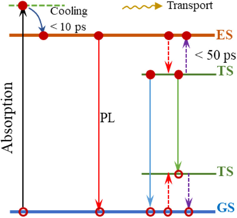
Similar study was employed to analyze double perovskite NCs [28]. First, the PL decay was fitted by a three-exponential function, and the obtained short-lived (50 ps) and middle-lived (1 ns) components were assigned to the sub-band-gap transition and electron–hole radiative recombination, respectively. The long-lived component (100 ns) was assigned to the emission from sub-band-gap state [139]. The fs TA was employed to further investigate the non-radiative process due to the low PLQY of NCs. As shown in Fig. 10(c), the observed decay times of 0.2 and 0.8 ps were assigned to the relaxation of hot holes and electrons, respectively. Furthermore, the 1.4 ps (40 ps) decay component was related to hole (electron) trapping. The author argued that the sub-band-gap TS may cause both radiative and non-radiative recombinations, which can be detected by both PL and TA.
It is interesting to note that exceptionally high PLQY () was observed in perovskite QDs [140], and this phenomenon was then confirmed by ultrafast TA spectroscopy studies. Kinetics of transient features are shown in Fig. 10(d), where exciton bleach (XB), photo-induced absorption (PA), and PL decay curves agreed well with each other; although PL decay did not resolve fast decay components due to its limited instrument response function. The decay time constants (and amplitudes) of () and () were obtained by TA analysis. The relatively high percentage of the 4.5 ns decay process was assigned to the electron−hole radiative recombination, and it can also be detected by PL. Similarly, kinetic agreement between slow decay processes of TA and PL signals in QDs was also observed by Li et al. [141].
B. Transient Photovoltage/Transient Photocurrent
The carrier lifetime of all-inorganic halide perovskite can also be investigated by other characterization techniques, including transient photovoltage (TPV), transient photocurrent (TPC) [49,51,124], time-resolved microwave conductivity (TRMC) [142], as well as intensity modulated photocurrent/photovoltage spectroscopy (IMPS/IMVS) [80]. The time calculated by the above measurements was found to be in the order of microseconds, much larger than those from TRPL and TA. We noticed that the reported studies were all employed in the PSCs, which means that the lifetime obtained may also be related to the external structure instead of the real dynamic process inside the perovskite film. Especially, for TPV, the difference between the extracted carrier lifetime and the intrinsic values was as high as 1 to 3 orders of magnitude, which has been quantitatively discussed by several researches [143–145] and will not be discussed here.
Figure 11.(a) TPC and (b) TPV studies for - and -based PSCs. Reprinted with permission [51]. (c) TPC and (d) TPV studies for film with or without layer. Reprinted with permission [124]. (e) TPC and (f) TPV studies for film with or without layer. Reprinted with permission [49].
We have reviewed the methods of exploring carrier dynamic processes by the PL technique and summarized the related results in recently reported all-inorganic halide perovskites. First, we discussed the bulk perovskite film, where the photo-generated carriers were mainly involved in recombination processes, i.e., radiative and non-radiative recombinations. Through fitting the power dependence of the SSPL integrated intensity and the excitation density, the mechanism of recombination can be estimated. More information about the carrier relaxation process can be deduced by utilizing the TRPL. Using the multiple exponential relation , the carrier lifetimes as well as their corresponding dynamic processes can be obtained, and the reported data simulated by the relation in all-inorganic halide perovskite materials were summarized in Table 1. It is found that for bulk thin film samples, two exponential terms were generally used, while for nanostructured materials, three exponential terms were needed, which indicates that the more complex the material structure, the more diversified the internal carrier recombination process. In addition, the excitation intensity dependency of PL intensity just after photoexcitation was also a way to study the nature of the radiative recombination.
Second, the PL properties of halide perovskite samples with TLs are investigated, where the dynamic process of photo-generated carriers is not only a recombination, but also a transfer to the TL. Compared with that of the pristine samples, the SSPL decreased sharply, and the TRPL curve became steeper due to the shorter carrier lifetime. To characterize the effect of TL on the transfer of photo-generated carriers in halide perovskite materials, the concept of transfer efficiency was introduced. We elaborated the relevant study reported in all-inorganic perovskite-based PSCs and sorted out the corresponding data in Table 3. In addition, the TRPL curve was also quantitatively fitted by a one-dimensional diffusion equation, through which other important transport characteristics, such as diffusion coefficient and length, can be simulated. It is found that the reported diffusion length in all-inorganic halide perovskite materials is in the range of 100 nm–10 μm, comparable or larger than those reported in hybrid perovskite samples.
Finally, we also briefly discussed other optoelectronic methods for studying carrier dynamics. Due to some limitations of instrument response, it is difficult to detect the very fast path by PL. Therefore, the combination of PL and TA is an effective choice to thoroughly investigate the photo-generated carrier dynamics. We also noticed that the carrier lifetime obtained by the TPV (TPC) test cannot accurately reflect the characteristics of carriers inside materials because of the influence from external structures. However, the qualitative conclusion is given for reference.
Overall, SSPL and TRPL are effective techniques to study the carrier dynamics of all-inorganic halide perovskites, and most researchers regard them as one of the necessary means for characterization. However, we note that most of the research groups only used the PL curve to obtain the corresponding carrier lifetime in all-inorganic halide perovskite materials [146–151]. There is neither further discussion on the external factors that will affect the carrier dynamics, such as growth method and doping, nor the internal physical explanation to the difference between the studied samples. Therefore, future investigation on these fields is still available and expected.