
Sh. G. Askerov, L. K. Abdullayeva, M. G. Hasanov. Study of electrophysical properties of metal–semiconductor contact by the theory of complex systems[J]. Journal of Semiconductors, 2020, 41(10): 102101
- Journal of Semiconductors
- Vol. 41, Issue 10, 102101 (2020)
Abstract
1. Introduction
Due to the fast development of the technology, the attempts at multifunctional uses of small-scale devices has significantly increased. When a metal and a semiconductor come into contact, the Schottky diode (SD), often called a “Schottky semiconductor diode”[
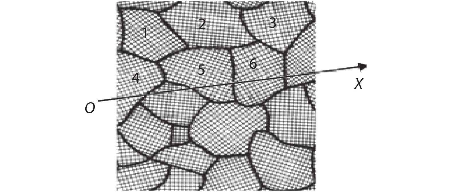
It is obvious that the homogeneous model does not fully describe the real situation, since in many practical cases the interface is inhomogeneous. The interface of a real MSC is heterogeneous, mainly due to the polycrystallinity of the metal. A homogeneous model cannot describe the processes occurring in an inhomogeneous contact, where the interface, based on emission parameters, is considered to be homogeneous in two dimensions.
We believe that all of the above problems are explainable if we apply the inhomogneous model[
There is an opinion that the structure and state of the semiconductor surface has a decisive influence on the operation of the MSC, which can be agreed upon with the polycrystalline structure of the semiconductor[
As is known from the literature, the microstructure of the film determines the important role of the metal[
As noted above, due to the mosaic microstructure of the metal of the interface, the MSC becomes inhomogeneous, and as a result the contact becomes a complex system.
When studying the contact, it is necessary to take into account the complexity of the system, which consists of the parallel connection of numerous homogeneous elementary subcontacts with different properties and parameters[
![]()
Figure 1.Microstructure of the surface of a polycrystalline metal.
For example, the barrier height (BH) with inhomogeneous interface can be expressed by the formula[
where
The temperature dependence of the current–voltage (I–V) characteristics is an effective physical method for studying the properties of a MSC[
According to the inhomogeneous model, the barrier height of systems consisting of two parallel-connected homogeneous diodes has a temperature dependence, even if the heights of the subdiode barriers do not depend on temperature, as it follows from the theory of complex systems[
where ФB(0) is the height of the contact barrier at T= 0, α is the temprature coefficient of the barrier height related with the inhomogeneity order of the interface that is expressed by the formula[
where ΔФ is the difference between heights of the potential barriers of the subdiodes, ω and 1 – ω are relative areas of the subdiodes, correspondingly. In the case of the homogeneous contact, when ΔФ= 0, α is equal to zero. In the case of the inhomogeneous contact according to Eq. (3), α≠ 0 and depends on ω and ΔФ. Other words in this case α is a function of microstructure.
2. Materials and methods
Temperature annealing is a technological factor affecting to the microstructure and thus the degree of homogeneity of the contact between the metal and the semiconductor. The study of the properties Ni–n/Si of the SD showed that the properties and parameters of the diodes substantially depend on the area and parameters of the annealing temperature. This means that the diode or ohmic behavior of the contact can be controlled by changing the parameters of the annealing temperature and the area of the contacts.
The saturation current of the SD determined before and after thermal annealing can be expressed by the following formulas[
Here IS1 and IS2 are the saturation currents before and after annealing, respectively, S1 and S2 are the areas of the contact, A1 and A2 are Richardson’s coefficients, ФB1and ФB2 are the heights of the barriers of SD before and after heat treatment. B is the emission parameter of the considered interface that is expressed by the formula
We assume that under the influence of heat treatment, the area of the ordered contact areas increases due to the combination of crystallites (ordered areas) and atoms located in the intercrystalline space. Apparently, thermal annealing is a technological factor that changes the number of subdiodes (n) of a complex system.
Since ∝1 ≠ ∝2, the saturation currents are not equal: IS1≠ IS2. As a consequence of this, the height of the barrier of the SD before and after heat treatment should not be equal to each other (ФB1≠ ФB2). This means that the difference in barrier heights for the same contact, measured by different authors, is a consequence of the uniqueness of the interface, which changes under the action of thermal annealing.
From the above it follows that ФB is a necessary, but insufficient parameter for the description of the emission properties of interfaces[
However, their product in the form of a correlation (6) can serve as a parameter of the interface, since it is constant for a given metal and semiconductor pair and does not depend on technological or design parameters such as thermal annealing or the size of contacts.
Given the correlation dependence (4), (5), for the direct current of saturation of SD, one can write the formula:
Here B is the main emission parameter of interface between the metal and the semiconductor and expresses the saturation current density per square of temperature. The study of the temperature dependence of the saturation current of the current-voltage characteristics showed that with increasing T the saturation current increases in such a way that B remains almost constant:
In Fig. 2 the dependence IS/ST2 is given on the temperature for TiCu–n/Si SD with different contact area: 3 × 10⁻⁶; 7 × 10⁻⁶; 14 × 10–6 cm2. On the ordinate axis IS/ST2 is given in the unit μA/(cm2·K2), on the axis abscissa – the temperature in K. As one can see from the figure in the temperature diapason of 298–373 K, IS/ST2 depends weakly on the temperature. Weak growth is likely due to the multiplier
![]()
Figure 2.(Color online) Dependence of
that demonstrates the influence of the inhomogeneity order of the interface. With a further increase of temperature 373–472 K, IS/ST2 increases significantly with the increase of T.
Apparently, this is due to the reconstruction of the microstructure of interface under the influence of the temperature exposure. According to Eq. (8), when
The new emission parameter B varies over a wide range depending on the nature and structure of the metal. Fig. 3 shows the dependence of IS/ST2 on the annealing temperature for the SD Al–n/Si with the area of 7 × 10⁻⁶ cm2. From the comparison of Figs. 2 and 3, it can be noted that at the room temperature for SD Ti Cu–n/Si with an area of S = 7 × 10⁻⁶ cm2, the value B = 11 μA/(cm2·K2), and in the case of SD Al–n/Si SD with the same area, the value B = 50 μA/(cm2·K2) is obtained.
![]()
Figure 3.(Color online) Dependence of
Thus, we can conclude that, depending on the nature of the metal, the emission parameter B varies in a wide range from 5.83 × 10⁻¹⁰ to 6.3 × 10⁻⁶ A/(cm2·K2) (Table 1).
From the foregoing, it can be concluded that metal plays a more active role in the electronic processes occurring in the MSC, and the polycrystallinity of the metal converts the contact into a complex system, where MSC consists of numerous elementary and homogeneous parallel connected subcontacts, the number of which varies due the parameters of thermo annealing and the contact area.
3. Conclusion
From the foregoing, we can conclude that in physical processes occurring in the contact of a metal with a single-crystal semiconductor, the metal plays a more active role than the semiconductor if the metal has a polycrystalline structure. The polycrystallinity of the metal translates the MSC into a complex system[
Schottky diodes made with the use of polycrystalline metals is a convenient object for checking the conclusions of the theory of complex systems. Many complex[
The use of Schottky diodes allows one to study a number of laws of a complex system with a change in the number of subcontacts.
Our study allowed us to draw the following conclusions:
1. It was shown that the height of the SD barrier with an inhomogeneous interface has a temperature dependence, even if the height of the barrier of sub-diodes is temperature independent, as follows from the theory of complex systems.
2. It is believed that ФB is a necessary but insufficient parameter for describing the emission properties of interfaces. Separately, both PV and A cannot perform the functions of the MSC parameter, since their values are a function of surface coordinates. However, their product in the form of correlation (6) can serve as an interface parameter, since it is constant for a given metal and semiconductor pair.
3. To describe the emission properties of MSCs, it is proposed to use a metal and a semiconductor B constant for the given pair, which expresses the density of the saturation current per square temperature. Parameter B varies over a wide range depending on the nature and structure of the metal.
4. It is proposed to study the nature of complex systems using SD. It is known that many complex phenomena are difficult to reproduce in the real world. However, the use of SD allows one to study a number of patterns of a complex system when changing the number of subcontacts.
References
[1]
[2]
[3]
[4] S G Askerov. A heterogeneous model of the MSC. Materials of the III All-Union Scientific Technical Seminar, 122(1984).
[5] V S Trush, I N Pohrelyuk, A H Luk'yanenko. Kinetic aspects of high-temperature interaction of titanium alloys with gaseous mediums. J Mod Technol Eng, 3, 92(2018).
[6] R Patra, S P Barik, P K Chaudhuri. Penny shaped crack in an infinite transversely isotropic piezoelectric layer under symmetrically applied line load. Adv Math Models Appl, 2, 117(2017).
[7] S Q Askerov, L K Abdullayeva, M H Hasanov. Origin of discrepancies in the experimental values of the barrier height at metal–semiconductor junctions. Semiconductors, 51, 620(2017).
[8] M K Hudait, S B Krupanidhi. Doping dependence of the barrier height and ideal of Au/n-GaAs Schottky diodes at low temperatures. Physica B, 307, 125(2001).
[9] K Saweta, S A Neeleshwar, N Arti. Current–voltage–temperature (
[10] I M Afandiyeva, Ş Altındal, L K Abdullayeva. Illumination dependent electrical characteristics of PtSi/n-Si(111) Schottky barrier diodes (SBDs) at room temperature. J Mod Technol Eng, 2, 43(2017).
[11]
[12] S G Askerov, L K Abdullayeva, M H Hasanov. The influence of the metal microstructure on the breakdown mechanism of Schottky diodes. J Mater Phys Chem, 1, 1(2018).
[13] I M Afandiyeva, Ş Altındal, L K Abdullayeva et al. Self-assembled patches in PtSi/n-Si (111) diodes. J Semicond, 39, 054002(2018).
[14] Ü Akın, Ö F Yüksel, O Pakma et al. A novel device behavior of Al/coronene/n-GaAs/inorganic based Schottky barrier diode. New Mater Compd Appl, 3, 15(2019).
[15] M Sistani, M A Luong, M I Den Hertog et al. Monolithic axial and radial metal–semiconductor nanowire heterostructures. Nano Lett, 18, 7692(2018).
[16] S H Lee, S W Lee, T Jeon et al. Efficient direct electron transfer via band alignment in hybrid metal–semiconductor nanostructures toward enhanced photocatalysts. Nano Energy, 63, 103841(2019).
[17] B Lu, X F Liu, Y P Gao et al. Berry phase in an anti-PT symmetric metal –semiconductor complex system. Opt Express, 27, 22237(2019).
[18] K W Cheng, S C Wang. Effects of complex agents on the physical properties of Ag–In–S ternary semiconductor films using chemical bath deposition. Mater Chem Phys, 115, 14(2009).
[19] Y Holovatch, R Kenna, S Thurner. Complex systems: Physics beyond physics. Eur J Phys, 38, 023002(2017).

Set citation alerts for the article
Please enter your email address
© Copyright 2018-2021 | Chinese Laser Press. All Rights Reserved 沪ICP备15018463号-20