
Shuai Yuan, Changran Hu, An Pan, Yuedi Ding, Xuanhao Wang, Zhicheng Qu, Junjie Wei, Yuheng Liu, Cheng Zeng, Jinsong Xia. Photonic devices based on thin-film lithium niobate on insulator[J]. Journal of Semiconductors, 2021, 42(4): 041304
- Journal of Semiconductors
- Vol. 42, Issue 4, 041304 (2021)
Abstract
1. Introduction
Compared to traditional microwave links, microwave photonic links have a series of advantages such as instantaneous broadband processing capability, light weight, low loss, anti-electromagnetic interference, etc., and in recent years, they have been widely used in radar and other fields. However, most of the current microwave photonic systems are built using discrete optoelectronic components, so there are shortcomings such as low integration, high link loss, large noise coefficient, which seriously hinders the performance of microwave photonic technology. So there is an urgent need to enable the on-chip integration of microwave photonic systems[
Research of integrated photonics has progressed rapidly in the last decade. Researchers have built low-loss optical waveguides, lasers, modulators, detectors on materials such as silicon[
Lithium niobate on insulator (LNOI) materials are structurally similar to SOI materials. It can be divided into three layers, the substrate layer (silicon), a low refractive index oxide layer (silicon dioxide) and a high refractive index device layer (lithium niobate film). Due to the high refractive index contrast between lithium niobate and silicon dioxide, thin-film lithium niobate waveguides allow for a strong limitation of the optical field and tight waveguide bending radii, thereby reducing the size of photonic devices. We believe that LNOI materials have the following advantages over silicon, indium phosphorus, silicon oxide, and silicon nitride materials.
(1) Due to the large refractive index difference between the waveguide core and the outer cladding, the dimensions of both SOI and InP waveguides are small, and there is a significant overlap between the inner mode and the waveguide sidewalls, which makes it difficult to reduce the scattering loss of light waves due to rough sidewalls.
(2) Si3N4 and SiO2 materials lack intrinsic electro-optical effects, and can only achieve modulation of optical phase through thermal-optical effects, so the optical switching speed realized on Si3N4 and SiO2 platform is slow (about sub-millisecond magnitude) with high power consumption.
(3) The refractive index contrast of the LNOI platform is high, which allows the construction of low-loss waveguides. The electro-optical effect of lithium niobate has femtosecond response speed, enabling ultra-wideband electro-optical modulators[
LNOI inherits the excellent material and optical properties of the bulk lithium niobate, and has the ability to integrate photonic devices similar to the SOI platform, which is very suitable for building a new generation of broadband, low-power microwave photonic RF front-end chips. In the second part, we will introduce the broadband electro-optical modulator, which is one of the core devices in the microwave photonic system. Its key parameters such as bandwidth, insertion loss, half-wave voltage and extinction ratio directly affect the performance of the whole microwave photonic link. In the third part, we will introduce the optical comb devices, including the electro-optical comb and the Kerr optical comb. In the fourth part, we will introduce how the coupling of multi-physics fields such as optical, acoustic, and electric fields can be achieved on thin-film lithium niobate chips, and discuss the possible applications. In the fifth part, we will introduce the thin film periodically poled lithium niobate (PPLN) waveguides, which play an important role in second harmonic generation (SHG), all-optical wavelength conversion and optical parametric amplification (OPA). In the sixth part, we will introduce the efficient coupling between thin-film lithium niobate waveguides and optical fibers, which is one of the prerequisites for the practical application of thin-film lithium niobate devices.
2. High-speed lithium niobate modulator
As early as 2007, Guarinoas et al. shows the electro–optically tunable microring resonators in thin film lithium niobate[
![]()
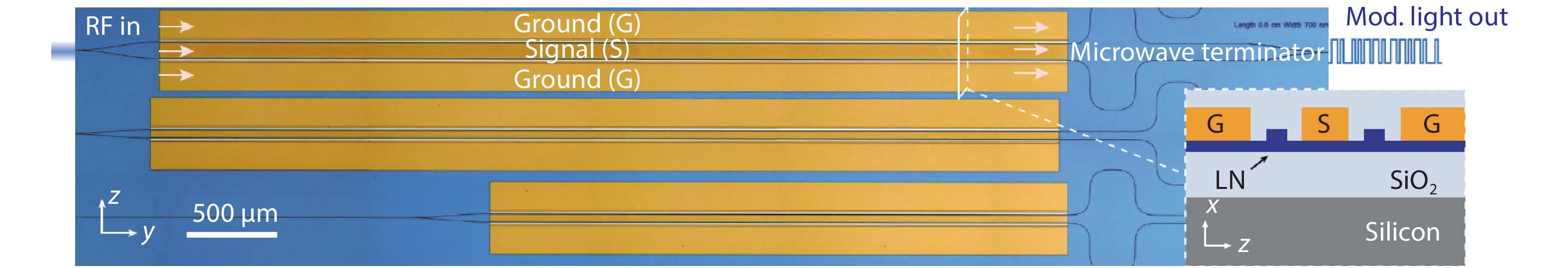
Figure 1.(Color online) The structure of the EO modulator made by Wang
In our group, the modulator is fabricated on a commercially available X-cut LNOI substrate (NANOLN) through a standard semiconductor process. The optical and the scanning electron microscope (SEM) images of the modulators are shown in Fig. 2.
![]()
Figure 2.(Color online) (a) Optical image of the modulators on the chip fabricated in our group. (b) SEM image of the electrode of the modulator. (c) SEM image of the cross section of the modulator’s waveguide. (d) SEM image of the area where the electrode stepping over the waveguide.
The transmission spectrum and the driving voltage test result of the modulator is indicated in Fig. 3(a). The measured free space range is about 3 nm and the VπL is about 2.75 V·cm. The measured EO response of the modulator are shown in Fig. 3(b), which exhibits a 3 dB EO bandwidth of about 40 GHz. In addition, the insertion loss of the whole device is about 3 dB when measured with high numerical aperture fiber (HNAF) and refractive index matching liquid.
![]()
Figure 3.(Color online) (a) The transmission spectrum of the modulator with and without the voltage applied. (b) The measured EO response of the modulator.
3. Optical frequency comb
Micro-resonator Kerr optical frequency combs characterized by discrete and equally spaced frequencies and high-repetition rate has provided miniaturised solutions for many applications, such as optical metrology, pulse shaping, light detection and ranging (LiDAR) and sources for quantum entanglement[
At present, almost all on-chip micro-resonator Kerr frequency comb generators rely on Kerr (third-order, χ(3)) nonlinear optical process. A continuous-wave laser source is injected in an optical micro-resonator which has a large Kerr nonlinear coefficient and low optical loss. They have been realized in various material platforms, including crystalline fluorides, Si3N4, SiO2, diamond, aluminium-gallium arsenide (AlGaAs), aluminium nitride (AlN) and Gallium phosphide (GaP)[
LN has been widely used in nonlinear optics, as it simultaneously possesses electro-optic (χ(2) = 30 pm/V) and Kerr (χ(3) = 1.6 × 10⁻²¹ m2/V2) nonlinearities[
As we all know, the above-mentioned platforms that have realized the generation of optical frequency comb such as silicon nitride usually possess large χ(3) but near zero χ(2) coefficients. As a result, they are restricted in the applications which required further on-chip manipulation of the generated combs. Due to the superior properties and low optical losses of LNOI, Wang et al. has achieved monolithic LN photonic circuits for Kerr frequency comb generation and modulation[
![]()
Figure 4.(Color online) (a) Monolithic integrated photonic circuit for frequency comb generation and manipulation[
Previous EO combs were generated through a sequence of discrete phase and amplitude modulators. They have been limited to narrow widths caused by a weak EO interaction strength and a lack of dispersion engineering in free-space systems. In Fig. 4(b), the EO comb with over 900 frequencies spaced by 10.453 GHz, spanning 80 nm over part of the telecommunication C-band, the entire L-band and part of the U-band is demonstrated leveraging the large χ(2) nonlinearity of LN, dispersion engineering, strong microwave and optical field overlap, and ultralow-loss optical waveguides. The device has a loaded Q up to 1.5 million. Furthermore, compared with the optical frequency comb produced by the Kerr effect, the main advantage of the electro-optical frequency comb is that its spectrum is not sensitive to the power of the input light, and there is no threshold for input power[
In addition, a soliton micro-comb in an LN microresonator is demonstrated by He et al.[
Our research group has also achieved some progress in the generation of on-chip optical frequency combs. The devices were fabricated on a 700-nm-thick x-cut congruent single-crystalline LN thin film sitting on a 1.8-µm-thick buried silicon dioxide layer (NANOLN). We utilize grating couplers for fiber-to-chip light coupling. As illustrated in Fig. 5, the micro-ring resonator has smooth surface with loaded factor up to 1.78 million. The inset shows TE fundamental mode. Fig. 6 shows the generated comb spectrum with a comb line spacing of ~ 200 GHz[
![]()
Figure 5.(Color online) SEM images of the microring resonator. (a) Coupling region of micro-ring. (b) Cross-section of waveguide. (c) Lorentz fitting of the resonance peak at 1572.6 nm, the
![]()
Figure 6.(Color online) Optical spectrum of a frequency comb pumped at 1549.927 nm.
4. Opto-electro-mechanical system on chip
One of the most important challenges in optical communications, sensing and imaging is controlling the propagation of light, which can be achieved from the basic principles of electromagnetism, either by varying the refractive index in a given medium, or by displacing the physical boundaries between media of different indices. However, the tuning range for the refractive index, provided by changes in electric fields[
LN is a kind of material with diversified properties such as piezoelectric, acousto-optical, electro-optical, nonlinear-optical, photorefractive, photovoltaic, photo-elastic and pyroelectric effect[
Amir H. Safavi-Naeini's Lab at Stanford University make important progress in the optomechanical crystal (OMC) device by demonstrating a photonic crystal resonator on LNOI that simultaneously supports high-Q optical and mechanical modes, where the mechanical modes are coupled piezoelectrically to microwaves. Optical quality factors above 300 000 and mechanical quality factors of 17 000 at cryogenic temperature are measured, leading to opto-mechanical coupling rates g0/2π ≈ 120 kHz by leveraging the photo-elastic effect. This LN OMC platform will open up opportunities for integrated ultra-low-power modulators, quantum microwave-to-optical converters and hybrid systems with densely integrated electrical, mechanical and optical elements[
In 2019, Piazza et al.[
![]()
Figure 7.(Color online) (a) SEM of the one-dimensional optomechanical crystal (OMC) design[
In 2019, Marko et al.[
5. Second-harmonic generation in PPLN waveguides
PPLN is widely used in second-harmonic generation (SHG)[
The group from The Ohio State University presented the poling electrodes as Fig. 8(a) shows. Fig. 8(b) provides a zoomed-in view of an electrode with a rounded tip. Fig. 8(c) is a schematic diagram of the polarization circuit. The signal generator generates a voltage pulse waveform, and then amplifies the voltage signal through a high-voltage amplifier. The +z direction of the PPLN adds a positive voltage, and the –z direction adds a negative voltage. Rs is the current limiting resistor, and the oscilloscope is used to monitor the polarization current in the process.
![]()
Figure 8.(Color online) (a) Schematic of poling electrodes and silicon nitride (SiN) strip on 700 nm thick x-cut MgO:LN thin film. (b) Zoomed-in view of poling electrode tip showing 160 nm chromium (Cr) on top of 100 nm SiO2. (c) Poling circuit; pulses generated from an arbitrary waveform generator (AWG) are amplified by a high voltage amplifier (HVA) and applied to a sample covered with silicone oil[
Fig. 9 shows the top-view SEM of a poled MgO-LN waveguide fabricated in our group after etching in hydrofluoric acid. It can be seen that the duty ratio of the inverted domain after polarization is about 1 : 1.
![]()
Figure 9.Top-view SEM of a poled MgO-LN mesa after etching in hydrofluoric acid.
In recent years, many groups have realized efficient second harmonic generation and optical parametric amplification on thin-film PPLN. For example, Harvard University used a nanostructured PPLN waveguide to demonstrate an ultrahigh normalized efficiency of 2600% W–1cm–2 for second-harmonic generation[
![]()
Figure 10.(Color online) Zoomed-in view of the SHG spectral response of the 1440-nm-wide device (solid curve), together with the theoretically predicted responses[
![]()
Figure 11.(Color online) SHG total conversion efficiency as a function of input power in the pump-depletion region. The inset shows the input-output power relation in the low-conversion limit[
Not only the PPLN waveguide can reach high efficiency SHG, the microring resonators based on PPLN can also achieve higher SHG efficiency than a traditional waveguide. For instance, the group from Yale University demonstrated high-efficiency SHG of 250 000%/W in dual-resonant, periodically poled z-cut LN microrings, where quasi-phase matching is realized by field-assisted domain engineering[
![]()
Figure 12.(Color online) (a) Numerical simulation of the poling period for QPM between the pump TE 00 and SH TM 00 modes using the Sellmeier equation for congruent LN. (b) Applied poling pulse shape. (c, d) False-color SEM images of a PPLN microring resonator etched with hydrofluoric acid and its zoomed-in view, revealing a poling duty cycle of ~35%[
![]()
Figure 13.(Color online) (a)
In summary, based on the realization of high SHG efficiency of thin-film PPLN, the published work has three extensions. One is to combine with microcavity to increase the frequency doubling slope efficiency by two orders of magnitude to achieve microwatt pumping. The second is to combine with temperature control to achieve tunable center wavelength. The third is to combine with waveguide dispersion engineering to achieve broadband frequency doubling.
At present, our group have produced an MgO-PPLN waveguide with SHG efficiency of 408% and absolute conversion efficiency of 8.32%, but there is still much room for improvement. In the next step, we will try different polarization periods to achieve the best quasi-phase matching.
6. Efficient edge coupling for LNOI
In traditional bulk lithium niobate platform, directly-coupling is widely used. But the huge gap between mode-field-diameter (MFD) of standard-single-mode-fiber (SSMF, ~10 µm) and integrated waveguide on LNOI (< 1µm) introduces a great coupling loss. The lensed taper fiber is used to reduce the coupling loss, but the experiments does not show a good result[
Figs. 14(a) and 14(b) illustrate the schematic structure of the proposed coupler by our group. We fabricated the coupler on a commercially available X-cut LNOI substrate (NANOLN) through standard semiconductor process. The top LN thin film is 500-nm thick. The measured transmission spectrum of the single coupler with HNAF is indicated in Fig. 15(a). At 1550 nm, the coupling loss is 0.54 and 0.59 dB/facet for TE and TM light and the polarization extinction ratio is low than 0.05 dB. The coupler has the coupling loss lower than 1 dB/facet for both TE and TM light at wavelengths longer than 1527 nm. It is expected that the coupler keeps lower than 1 dB/facet in the whole C+L-band (1530 to 1625 nm) according to the curve trend of the transmission spectrum. Comparatively, the coupling loss between edge coupler and SSMF (~10 µm) is 5.7 dB at 1550 nm for TE mode.
![]()
Figure 14.(Color online) (a) Structure of the edge coupler. (b) Overhead view of the edge coupler[
![]()
Figure 15.(Color online) (a) Transmission spectrum of the fabricated single coupler. (b) Coupling loss versus different tip widths of the lower LN inversed taper (TE mode)[
Couplers with various tip widths of the lower LN inversed taper were fabricated and tested. The simulated and measured coupling loss at 1550 nm versus different tip widths taper were shown in Fig. 15(b). As expected, the loss rises when the tips get wider, while the loss is still as low as 0.72 dB when the tip width reaches 400 nm. Comparing with the simulation result, the measured additional loss of the coupler might come from the imperfections induced in fabrication process.
7. Conclusion
The recent developments of photonic devices on the LNOI platform were reviewed. A variety of key building blocks for highly integrated photonic integrated circuits (PICs) have been established on this platform. Apart from the extraordinary electro-optical modulation and optical nonlinear generation characteristics, the excellent piezoelectric and acousto-optic properties of LNOI have also been demonstrated in opto-electro-mechanical systems. Furthermore, edge couplers consist of bilayer taper and cladding waveguide have been used to provide efficient fiber-to-chip coupling with loss lower than 1 dB/facet in the whole C+L-band.
However, a few challenges need to be overcome to make LNOI a commercially attractive and competitive integrated optical platform. (1) Systems on LNOI. Despite the great success in electric-optical and nonlinear devices, LN’s indirect bandgap limits its applications in light sources and photodetectors. Hybrid integration of III–V and Ge optical circuits on LNOI seems to be one of the most promising ways. (2) The limited wafer sizes and high cost per wafer, makes LNOI less competitive as compared with a more mature and cost-efficient wafer platform such as SiN and SOI. Whether LNOI could be widely adopted as a fundamental photonic integration platform is still hard to say. The demonstration of hybrid Si and LN MZI modulator shows another way as integrating local islands of thin film LN onto SOI. (3) Most of the LNOI fabrication techniques are only suitable for prototyping of optical devices in academic laboratories, such as electron-beam lithography and focused ion beam milling, which are incapable of mass production of LNOI-based devices. High performance LNOI optical circuits based on photolithograghy techniques could be expected, with improved photonic designs.
Acknowledgements
This work is supported by the National Key Research and Development Program of China (2019YFB2203800) and the National Natural Science Foundation of China under Grant No. 61835008, 61905079, and 61905084. We thank the Center of Micro-Fabrication and Characterization (CMFC) of WNLO and the Center for Nanoscale Characterization & Devices (CNCD), WNLO of HUST for the facility support.
References
[1] D Marpaung, C Roeloffzen, R Heideman et al. Integrated microwave photonics. Laser Photonics Rev, 7, 506(2013).
[2] W N Ye, Y L Xiong. Review of silicon photonics: History and recent advances. J Mod Opt, 60, 1299(2013).
[3] D Thomson, A Zilkie, J E Bowers et al. Roadmap on silicon photonics. J Opt, 18, 073003(2016).
[4] J J G M van der Tol, Y Q Jiao, L F Shen et al. Indium phosphide integrated photonics in membranes. IEEE J Sel Top Quantum Electron, 24, 1(2018).
[5] C Wang, M Zhang, B Stern et al. Nanophotonic lithium niobate electro-optic modulators. Opt Express, 26, 1547(2018).
[6] C Wang, M Zhang, X Chen et al. Integrated lithium niobate electro-optic modulators operating at CMOS-compatible voltages. Nature, 562, 101(2018).
[7] Y He, Q F Yang, J W Ling et al. Self-starting bi-chromatic LiNbO3 soliton microcomb. Optica, 6, 1138(2019).
[8] Y Sua, J Y Chen, Y P Huang. Ultra-wideband and high-gain parametric amplification in telecom wavelengths with an optimally mode-matched PPLN waveguide. Opt Lett, 43, 2965(2018).
[9] T J Wang, C H Chu, C Y Lin. Electro-optically tunable microring resonators on lithium niobate. Opt Lett, 32, 2777(2007).
[10] J Chiles, S Fathpour. Mid-infrared integrated waveguide modulators based on silicon-on-lithium-niobate photonics. Optica, 1, 350(2014).
[11] V E Stenger, J Toney, A PoNick et al. Low loss and low vpi thin film lithium niobate on quartz electro-optic modulators. European Conference on Optical Communication (ECOC), 1(2017).
[12]
[13] C Wang, M Zhang, M Yu et al. Monolithic lithium niobate photonic circuits for Kerr frequency comb generation and modulation. Nat Commun, 10, 978(2019).
[14] M X Li, J W Ling, Y He et al. Lithium niobate photonic-crystal electro-optic modulator. Nat Commun, 11, 4123(2020).
[15] S Han, L Cong, Y K Srivastava et al. All-dielectric active terahertz photonics driven by bound states in the continuum. Adv Mater, 31, e1901921(2019).
[16] M Xu, M He, H Zhang et al. High-performance coherent optical modulators based on thin-film lithium niobate platform. Nat Commun, 11, 3911(2020).
[17] T J Kippenberg, R Holzwarth, S A Diddams. Microresonator-based optical frequency combs. Science, 332, 555(2011).
[18] T Herr, V Brasch, J D Jost et al. Temporal solitons in optical microresonators. Nat Photonics, 8, 145(2014).
[19] P Marin-Palomo, J N Kemal, M Karpov et al. Microresonator-based solitons for massively parallel coherent optical communications. Nature, 546, 274(2017).
[20] R DeSalvo, A A Said, D J Hagan et al. Infrared to ultraviolet measurements of two-photon absorption and
[21] M Zhang, C Wang, R Cheng et al. Monolithic ultra-high-Q lithium niobate microring resonator. Optica, 4, 1536(2017).
[22] M Zhang, B Buscaino, C Wang et al. Broadband electro-optic frequency comb generation in a lithium niobate microring resonator. Nature, 568, 373(2019).
[23] A Pan, C R Hu, C Zeng et al. Fundamental mode hybridization in a thin film lithium niobate ridge waveguide. Opt Express, 27, 35659(2019).
[24] K Liu, C Ye, S Khan et al. Review and perspective on ultrafast wavelength-size electro-optic modulators. Laser Photonics Rev, 9, 172(2015).
[25] A Faraon, J Vučković. Local temperature control of photonic crystal devices via micron-scale electrical heaters. Appl Phys Lett, 95, 043102(2009).
[26] B R Bennett, R A Soref, J A del Alamo. Carrier-induced change in refractive index of InP, GaAs and InGaAsP. IEEE J Quantum Electron, 26, 113(1990).
[27] C Baker, W Hease, D T Nguyen et al. Photoelastic coupling in gallium arsenide optomechanical disk resonators. Opt Express, 22, 14072(2014).
[28] L Midolo, A Schliesser, A Fiore. Nano-opto-electro-mechanical systems. Nat Nanotechnol, 13, 11(2018).
[29] R S Weis, T K Gaylord. Lithium niobate: Summary of physical properties and crystal structure. Appl Phys A, 37, 191(1985).
[30]
[31] S B Gong, G Piazza. Design and analysis of lithium–niobate-based high electromechanical coupling RF-MEMS resonators for wideband filtering. IEEE Trans Microw Theory Tech, 61, 403(2013).
[32] G Poberaj, H Hu, W Sohler et al. Lithium niobate on insulator (LNOI) for micro-photonic devices. Laser Photonics Rev, 6, 488(2012).
[33] W T Jiang, R N Patel, F M Mayor et al. Lithium niobate piezo-optomechanical crystals. Optica, 6, 845(2019).
[34] L T Cai, A Mahmoud, M Khan et al. Acousto-optical modulation of thin film lithium niobate waveguide devices. Photonics Res, 7, 1003(2019).
[35] L B Shao, M J Yu, S Maity et al. Microwave-to-optical conversion using lithium niobate thin-film acoustic resonators. Optica, 6, 1498(2019).
[36]
[37] J T Nagy, R M Reano. Reducing leakage current during periodic poling of ion-sliced x-cut MgO doped lithium niobate thin films. Opt Mater Express, 9, 3146(2019).
[38] C Wang, C Langrock, A Marandi et al. Ultrahigh-efficiency wavelength conversion in nanophotonic periodically poled lithium niobate waveguides. Optica, 5, 1438(2018).
[39] Y F Niu, C Lin, X Y Liu et al. Optimizing the efficiency of a periodically poled LNOI waveguide using
[40] A Rao, A Rao, A Rao et al. Actively-monitored periodic-poling in thin-film lithium niobate photonic waveguides with ultrahigh nonlinear conversion efficiency of 4600 %W−1cm−2. Opt Express, 27, 25920(2019).
[41] J J Lu, J B Surya, X W Liu et al. Periodically poled thin-film lithium niobate microring resonators with a second-harmonic generation efficiency of 250, 000%/W. Optica, 6, 1455(2019).
[42] J Y Chen, Z H Ma, Y Sua et al. Ultra-efficient frequency conversion in quasi-phase-matched lithium niobate microrings. Optica, 6, 1244(2019).
[43] D Pohl, M R Escalé, M Madi et al. An integrated broadband spectrometer on thin-film lithium niobate. Nat Photonics, 14, 24(2020).
[44] N Yao, N Yao, J X Zhou et al. Efficient light coupling between an ultra-low loss lithium niobate waveguide and an adiabatically tapered single mode optical fiber. Opt Express, 28, 12416(2020).
[45] I Krasnokutska, J L J Tambasco, A Peruzzo. Nanostructuring of LNOI for efficient edge coupling. Opt Express, 27, 16578(2019).
[46] L Y He, L Y He, M Zhang et al. Low-loss fiber-to-chip interface for lithium niobate photonic integrated circuits. Opt Lett, 44, 2314(2019).
[47] Y Pan, S H Sun, M Y Xu et al. Low fiber-to-fiber loss, large bandwidth and low drive voltage lithium niobate on insulator modulators. Conference on Lasers and Electro-Optics, JTh2B.10(2020).
[48]


Set citation alerts for the article
Please enter your email address

© Copyright 2018-2021 | Chinese Laser Press. All Rights Reserved 沪ICP备15018463号-20