• Photonics Research
  • Vol. 11, Issue 3, 476 (2023)
Xiaoxian He1, Xiangru Wang1、*, Yulin Zhao2, Rusheng Zhuo1, and Feng Liang2
Author Affiliations
  • 1School of Optoelectronic Science and Engineering, University of Electronic Science and Technology of China, Chengdu 610054, China
  • 2School of Physics, University of Electronic Science and Technology of China, Chengdu 610054, China
  • show less
    DOI: 10.1364/PRJ.482956 Cite this Article Set citation alerts
    Xiaoxian He, Xiangru Wang, Yulin Zhao, Rusheng Zhuo, Feng Liang. Field programmable topological edge array[J]. Photonics Research, 2023, 11(3): 476 Copy Citation Text show less
    Design principle of FPTEA. (a) Schematic of the programmable integrated topological device. The states of each programmable unit cell are controlled by an external field such as electrical, optical, or thermal field. After a beam is coupled into FPTEA, the valley-protected edge modes appear at the interface between two inversion broken lattices. (b) Three states of FPTEA lattice and the corresponding three-dimensional LC distribution. (c) Band dispersion diagram of the hexagram (blue dashed line) and AU/AD states (solid red line); there is a clear band gap from 0.326 to 0.346 (c/a) for AU/AD states. (d) Phase distribution of Ez and Poynting power flow of the modes at the K (K′) valley and band 1 (2) for the AU state, respectively. (e) Relationship of nontrivial valley bandgap and birefringence of LC. With the increase of birefringence, the topological photonic system demonstrates central frequency redshifting and wider nontrivial bandgap.
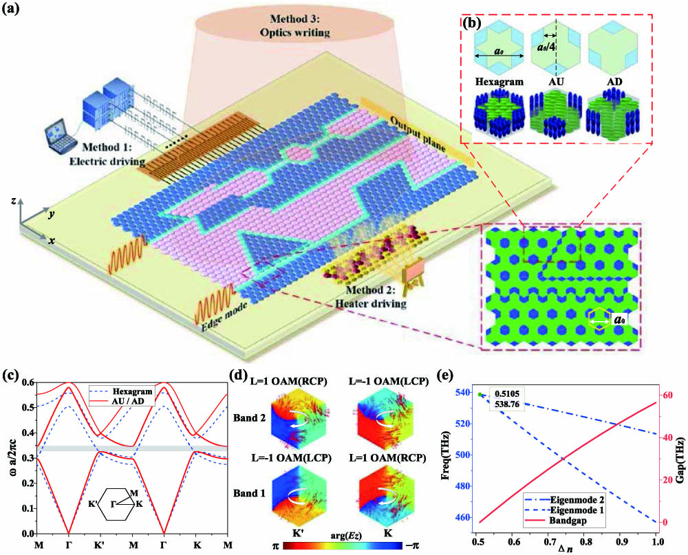
    Fig. 1. Design principle of FPTEA. (a) Schematic of the programmable integrated topological device. The states of each programmable unit cell are controlled by an external field such as electrical, optical, or thermal field. After a beam is coupled into FPTEA, the valley-protected edge modes appear at the interface between two inversion broken lattices. (b) Three states of FPTEA lattice and the corresponding three-dimensional LC distribution. (c) Band dispersion diagram of the hexagram (blue dashed line) and AU/AD states (solid red line); there is a clear band gap from 0.326 to 0.346 (c/a) for AU/AD states. (d) Phase distribution of Ez and Poynting power flow of the modes at the K (K) valley and band 1 (2) for the AU state, respectively. (e) Relationship of nontrivial valley bandgap and birefringence of LC. With the increase of birefringence, the topological photonic system demonstrates central frequency redshifting and wider nontrivial bandgap.
    Valley-protected topological edge states. (a) Zigzag type 1 interface and the corresponding band diagram. The black dot lines represent the bulk modes, the red and blue dotted lines indicate the valley-protected edge states from valley K and K′, and the corresponding |Ez| field distribution and Poynting vector distribution (red arrows) at points A and B were given. (b) Zigzag type 2 interface and the corresponding band diagram. The black dot lines represent the bulk modes, the red and blue dotted lines indicate the valley-protected edge states from valley K and K′, and the corresponding |Ez| field distribution and Poynting vector distribution (the red arrows) at points C and D were given. (c) Armchair interface and corresponding band diagram with two types of modes.
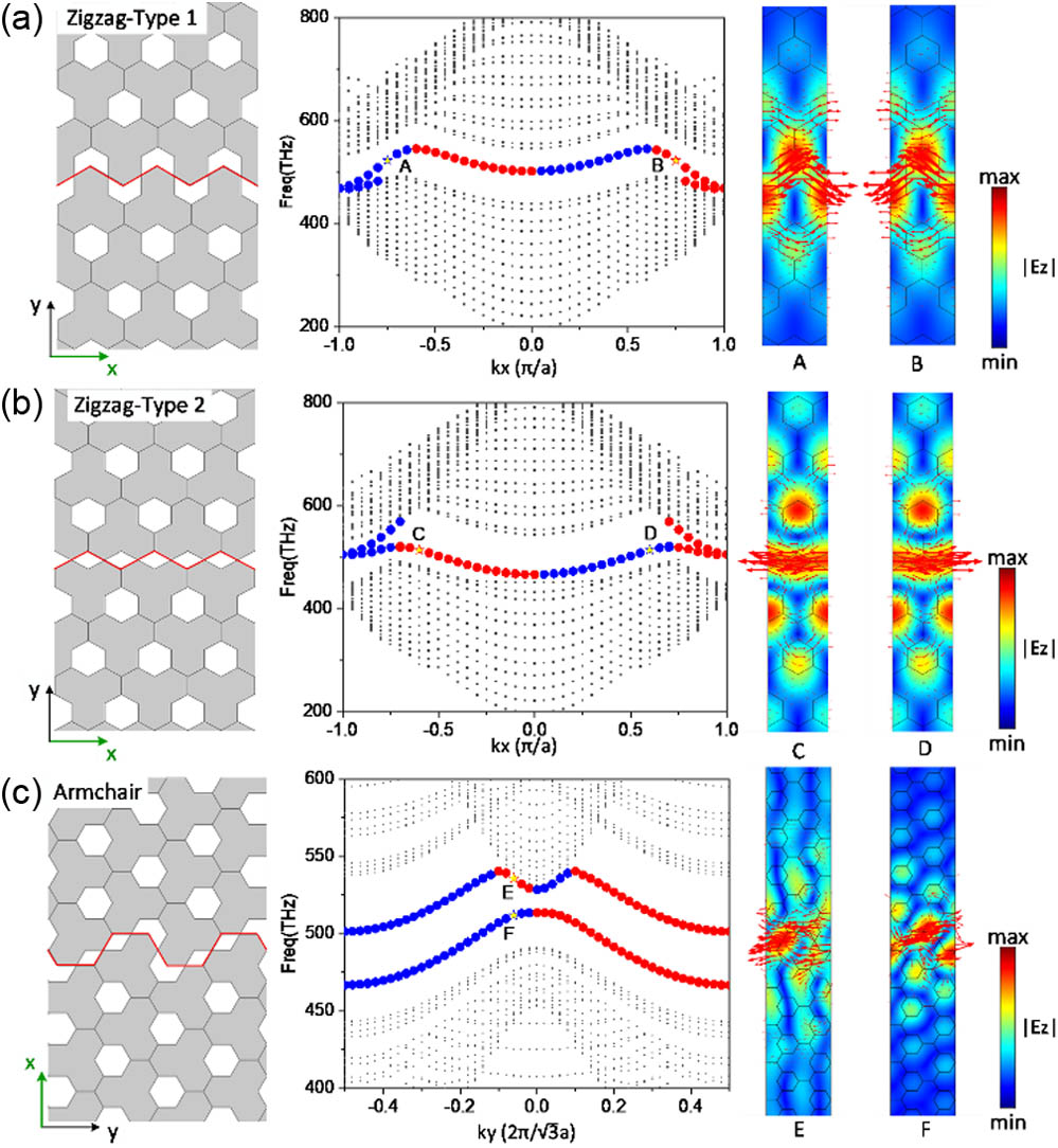
    Fig. 2. Valley-protected topological edge states. (a) Zigzag type 1 interface and the corresponding band diagram. The black dot lines represent the bulk modes, the red and blue dotted lines indicate the valley-protected edge states from valley K and K, and the corresponding |Ez| field distribution and Poynting vector distribution (red arrows) at points A and B were given. (b) Zigzag type 2 interface and the corresponding band diagram. The black dot lines represent the bulk modes, the red and blue dotted lines indicate the valley-protected edge states from valley K and K, and the corresponding |Ez| field distribution and Poynting vector distribution (the red arrows) at points C and D were given. (c) Armchair interface and corresponding band diagram with two types of modes.
    Simulated results for the transmission of programmable topological paths. Schematic and |Ez| field distribution at 500 THz of (a) 0°, (b) 30°, (c) 60°, (d) 90°, (e) 120°, and (f) 150° topological propagation path; (g) transmission of a field over a zigzag type 2 topological path with random defects; (h), (i) Simulation of unidirectional coupling in a zigzag type 2 interface by controlling the chirality of a circularly polarized source at 500 THz. To simplify, a right-circularly polarized (RCP) or left-circularly polarized (LCP) dipole source is considered to generate a clockwise/anticlockwise phase vortex. (j) Schematic and distribution of |Ez| field at 500 THz for a multi-interface path. (k) Transmittance results for six different interface conditions, i.e., no interface (gray curve), zigzag-type 1 interface along straight domain wall (yellow curve), zigzag-type 2 interface along straight domain wall (purple curve), armchair interface along straight domain wall (green curve), waveguide of (g), and multi-interface path of (j).
    Fig. 3. Simulated results for the transmission of programmable topological paths. Schematic and |Ez| field distribution at 500 THz of (a) 0°, (b) 30°, (c) 60°, (d) 90°, (e) 120°, and (f) 150° topological propagation path; (g) transmission of a field over a zigzag type 2 topological path with random defects; (h), (i) Simulation of unidirectional coupling in a zigzag type 2 interface by controlling the chirality of a circularly polarized source at 500 THz. To simplify, a right-circularly polarized (RCP) or left-circularly polarized (LCP) dipole source is considered to generate a clockwise/anticlockwise phase vortex. (j) Schematic and distribution of |Ez| field at 500 THz for a multi-interface path. (k) Transmittance results for six different interface conditions, i.e., no interface (gray curve), zigzag-type 1 interface along straight domain wall (yellow curve), zigzag-type 2 interface along straight domain wall (purple curve), armchair interface along straight domain wall (green curve), waveguide of (g), and multi-interface path of (j).
    Demonstration of realization of FPTEA device based on direct electric driving. (a) Three-dimensional design of an FPFEA device with four units controlled by an FPGA platform. (b) Sandwich structure with multilayers of a unit cell. (c) Distribution of LC molecules under different voltage conditions of V0 and Vs.
    Fig. 4. Demonstration of realization of FPTEA device based on direct electric driving. (a) Three-dimensional design of an FPFEA device with four units controlled by an FPGA platform. (b) Sandwich structure with multilayers of a unit cell. (c) Distribution of LC molecules under different voltage conditions of V0 and Vs.
    Demonstration of realization of FPTEA device based on direct thermal inducing. (a) Three-dimensional structure with multilayers of a lattice. (b) Local schematic of the heating layer of FPTEA device. (c) Two states of LC molecules under two temperatures T1 and T2.
    Fig. 5. Demonstration of realization of FPTEA device based on direct thermal inducing. (a) Three-dimensional structure with multilayers of a lattice. (b) Local schematic of the heating layer of FPTEA device. (c) Two states of LC molecules under two temperatures T1 and T2.
    Demonstration of realization of FPTEA device based on indirect UV writing. (a) Realization progress of reconfigurable topological PhCs based on optical field control. Two masks for UV light (365 nm) and visible light (445 nm) are sequentially switched to irradiate the azobenzene materials, and a device for two different input frequencies with two kinds of paths is realized. (b) Two states of photoinduced azobenzene material and the corresponding states of LC molecules.
    Fig. 6. Demonstration of realization of FPTEA device based on indirect UV writing. (a) Realization progress of reconfigurable topological PhCs based on optical field control. Two masks for UV light (365 nm) and visible light (445 nm) are sequentially switched to irradiate the azobenzene materials, and a device for two different input frequencies with two kinds of paths is realized. (b) Two states of photoinduced azobenzene material and the corresponding states of LC molecules.
    Illustration of three typical optical devices with topological edge modes. (a) LC distribution structure, (b) field distribution, and (c) simulated transmission curve of a programmable beam splitter. (d) Design of a programmable true time delayer and (e) the corresponding field distribution. (f) Calculated results of transmission time of the double Z-shaped and straight paths. (g) Structure of a programmed interferometer. (h) Field distributions of four interferometers with different signal path lengths of 56a/3, 54a/3, 52a/3, and 50a/3, respectively. (i) Probed interference phases at four probe points corresponding to cases h1 to h4 under different frequencies.
    Fig. 7. Illustration of three typical optical devices with topological edge modes. (a) LC distribution structure, (b) field distribution, and (c) simulated transmission curve of a programmable beam splitter. (d) Design of a programmable true time delayer and (e) the corresponding field distribution. (f) Calculated results of transmission time of the double Z-shaped and straight paths. (g) Structure of a programmed interferometer. (h) Field distributions of four interferometers with different signal path lengths of 56a/3, 54a/3, 52a/3, and 50a/3, respectively. (i) Probed interference phases at four probe points corresponding to cases h1 to h4 under different frequencies.
    Xiaoxian He, Xiangru Wang, Yulin Zhao, Rusheng Zhuo, Feng Liang. Field programmable topological edge array[J]. Photonics Research, 2023, 11(3): 476
    Download Citation