Valley Hall topological photonic crystals, inspired by topological insulators in condensed matter physics, have provided a promising solution to control the flow of light. Recently, the dynamic manipulation property of topological photonic crystals has been widely studied. Here, we propose a novel solution for programmable valley photonic crystals, called field programmable topological edge array (FPTEA), based on the field reorientation property of nematic liquid crystals and robust valley-protected edge modes. FPTEA is composed of an array of graphene-like lattices with symmetry, in which the birefringence of liquid crystal is larger than 0.5105. Due to the dielectric anisotropy of liquid crystals being sensitive to external fields such as light, heat, electric, and magnetic fields, each lattice is tunable, and the topological propagation routes and even the lattice parameters can be dynamically changed while changing the distribution of external fields. We numerically demonstrate three methods of composing an FPTEA device to design arbitrary passive optical devices by electric driving, thermal inducing, or UV writing. These results show the great application potential of liquid crystals in topological photonic crystals, and enrich the design of programmable integrated topological devices with broad working bandwidth ranging from microwave to visible light.
1. INTRODUCTION
Photonic crystals (PhCs) have played a significant role in the field of optical field manipulation (OFM). Unlike the traditional OFM scheme in the displacement space, PhCs are governed by the band dispersion theory of periodic dielectric material being discussed in the reciprocal space. By regulating band dispersion, PhCs have demonstrated non-diffraction propagation [1,2], anomalous refraction [3,4], self-collimation [5,6], and other interesting phenomena. Introducing the concept of topology into PhCs governed by Maxwell’s equation results in various analogical nontrivial features, attracting dramatically increasing interest in its nontrivial edge mode, and shows vital potential from optical fundamentals to practical applications such as topological lasers [7,8], topological waveguides [9,10], and topological optical localization [11–14]. Recently, dielectric materials have been used to construct topological valley Hall PhCs with breaking inversion symmetry. In further, valley-protected edge modes with fascinating phenomena have been demonstrated, such as a notable vortex nature in eigenstates, valley-selective excitation, and reflection immunity to sharp corners [15–19].
Until now, the dispersion features of most nontrivial PhCs have been invariable after electromagnetic design in terms of geometry, material, and fabrication, although a few solutions on the acoustic spectrum were reported by mechanical deformation, positive–intrinsic–negative (PIN) diode switch, and thermal phase changing where the typical size of a unit cell is millimeters or even larger [20–22]. Focusing on tunable dielectric materials, they are classified into thermal-induced phase-changing [22], Kerr effect nonlinearity [23], free-carrier excitation [24], liquid crystal (LC) reorientation [25], and so on. Therein, LC is a widely used commercial soft material with obvious potential in topological photonics because of such advantages as large tunable refractive index, low driving voltage, wide spectrum response from microwave to visible, and less power consumption [26–28]. In addition to adjusting the band position of topological PhCs by the tunable refractive index of LCs [25,29–32], a theoretical model of a spiral LC-filled Floquet topological insulator was presented to demonstrate an analogical quantum Hall effect resulting from breaking time-reversal symmetry [33].
The design and synthesis of novel LC molecules has been highly researched. The latest LCs with high birefringence () have been synthesized in accordance with –electron conjugation, functional groups, and compound structures [34–37]. But this latest LC material has not been exploited in topological PhCs.
Sign up for Photonics Research TOC. Get the latest issue of Photonics Research delivered right to you!Sign up now
To be analogous to field programmable gate array (FPGA), which is widely used and supports arbitrary logic circuit programming electric circuit platforms [38], a universally programmable integrated topological devices (UPITD) with couplings of tunable units is expected to program arbitrary one-way path, directional intersection, splitter, combiner, interferometer, and so on. To support a solution of UPITD, a nematic LC-filled device called a field programmable topological edge array (FPTEA) was proposed to generate tunable robust valley-protected edge modes and support in situ field programmable functions, including low risk, low incremental cost, and flexible reconfiguration. As a topological phase-changing material, LCs with two states are arranged in a hexagonal lattice to break inversion symmetry and emulate the topological valley Hall effect. Valley-protected edge modes emerge at the interface between two inverse lattices. By controlling the arrangement states of LCs in each unit lattice, the valley-protected edge modes will propagate along arbitrary paths to achieve field programmability. Since the reorientation of LC is determined by an external field, three practical methods including electric driving, thermal inducing, and mask-controlled UV writing are suggested to compose the realization of the FPTEA device. In addition, three typical prototypes of the beam splitter, true time delayer, and interferometer are numerically demonstrated to verify the programmability of FPTEA.
2. DESIGN
A. Architecture
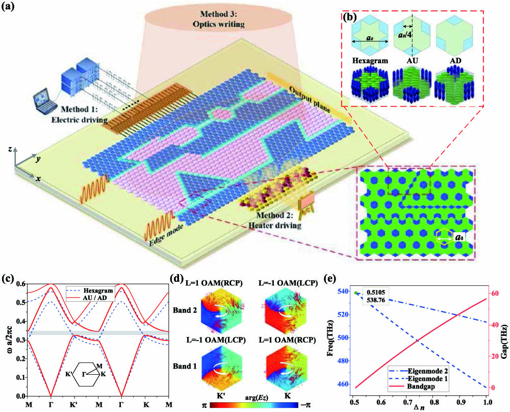
The proposed FPTEA consists of programmable unit cells arranged in a graphene-like lattice with lattice constant of , as shown in Fig. 1(a). An electromagnetic wave is coupled into the FPTEA device from the left side input port, and edge modes appear at the interface (shown in light blue) between two inversion broken lattices (shown in blue and pink). From the zoom-in picture of Fig. 1(a), the detailed lattice arrangement is presented with at least two kinds of zigzag interfaces, two sides of which are all hexagon lattices filling with LCs. Furthermore, the original hexagon lattice consists of an inner hexagram and six outer end-to-end rhombi to be symmetric, as shown in the upper-left picture of Fig. 1(b). The inner hexagram is filled with planar-aligned (homogeneous) LCs. The alignment of LCs in the outer six circular arranged rhombi is driven by external field, and they are arranged as homogeneous or homeotropic. Two kinds of hexagon lattice are easily obtained: arrow upward (AU) and arrow downward (AD), with symmetry and inversion symmetry broken, where the ellipsoids in dark blue and green in Fig. 1(b) represent vertical and homogenous aligned LCs, respectively. Since the states of each lattice are determined by the external field, the propagation path of the valley-protected edge modes could be programmed. Three possible methods of electric driving, optics driving, and heater driving are proposed and shown in Fig. 1 to realize the field programmability of the FPTEA device. For electric driving or a thermal inducing scheme, each lattice has two independent wires connected to the output of a driving system to generate a specific electrical or thermal field. From a personal computer, a programmed topological PhC pattern is synthesized to datum packages and mapped into FPTEA lattices at arbitrary times via the output wire. For the optical writing methods, the reorientation of LC molecules is achieved by a rewritable and double wavelength-sensitive azobenzene material, and the topological PhC patterns are written to the FPTEA device by pairs of amplitude masks and two spectrum light sources. To better understand the details, the three driving schemes are further discussed in Section 3.
Figure 1.Design principle of FPTEA. (a) Schematic of the programmable integrated topological device. The states of each programmable unit cell are controlled by an external field such as electrical, optical, or thermal field. After a beam is coupled into FPTEA, the valley-protected edge modes appear at the interface between two inversion broken lattices. (b) Three states of FPTEA lattice and the corresponding three-dimensional LC distribution. (c) Band dispersion diagram of the hexagram (blue dashed line) and AU/AD states (solid red line); there is a clear band gap from 0.326 to 0.346 () for AU/AD states. (d) Phase distribution of and Poynting power flow of the modes at the () valley and band 1 (2) for the AU state, respectively. (e) Relationship of nontrivial valley bandgap and birefringence of LC. With the increase of birefringence, the topological photonic system demonstrates central frequency redshifting and wider nontrivial bandgap.
On the physical model of uniaxial crystal, the electromagnetic wave propagating in LC is classified as two orthogonal waves: transverse electric wave TE (, ) and transverse magnetic wave TM (). Here, we restrict the discussion to the TM modes. The -component electromagnetic wave along the LC device is governed by Maxwell’s equation on anisotropic material: where is the relative anisotropic permittivity tensor, is the speed of light in vacuum, and is the angular frequency of TM wave. The magnetic field is given by the Faraday relation , where the magnetic permeability is vacuum permeability . As a uniaxial crystal, the permittivity tensor of LC material in the homogeneous and homeotropic states are and , respectively. The elements and are the permittivity on the given axis determined by the LC molecules’ temperature and central bridge band. Meanwhile, a typical identical equation between relative permittivity and refractive index . Note that, for historical reasons, relative permittivity and refractive index are independently used in the microwave and optics fields, respectively. On the current terahertz spectrum, the rule or habit of using relative permittivity or refractive index is not specific from now on. Indeed, the defining equation is identical. The birefringence of the LC we used in the FPTEA scheme is from Ref. [37]: , i.e., the dielectric anisotropy is and .
Based on the numerical finite element methods (FEM), the band diagram of FPTEA is obtained by the commercial software Multiphysics COMSOL, as shown in Fig. 1(c). When the FPTEA lattice is in the hexagram state, Dirac degeneracies are apparently at the and points in the blue dotted energy dispersion curves due to the symmetry. By controlling the two alinement states of LC hopingly arranged in six rhombus subdomains, the symmetry of the lattice is broken from symmetry to symmetry, and it could be on the states of AU or AD. As a comparison, the initial Dirac degeneracy is broken at the () valley and opens a bandgap shown in solid red lines in Fig. 1(c). Quantitatively, if the lattice constant is assumed 197 nm, the band gap is 30.85 THz near the Dirac point (). Further, the phase distribution and Poynting flow of the TM wave ( component) at the (left column) and (right column) valley for the AU state are shown in the color map and red arrow of Fig. 1(d). On the () column representing a momentum state, the left-handed circular polarization (LCP) and right-handed circular polarization (RCP) are the eigenmode distributions of band 2 (1) and band 1 (2), respectively. For the AD state, the chirality of every eigenmode is opposite to the AU state on the valley.
Furthermore, the topological bandgap is dependent on the birefringence of the filling LC. The nontrivial valley bandgap appears on the condition of larger birefringence than 0.5105. In Fig. 1(e), the eigenmode frequency and width of the nontrivial valley bandgap are plotted in blue dashed lines and solid red lines on the condition of . With the increase of birefringence, the topological photonic system demonstrates central frequency redshifting and wider nontrivial bandgap.
B. Valley-Projected Edge Modes
To verify the nontrivial topological character of the photonic states in the FPTEA lattice, valley-Chern index of each photonic band can be calculated by the following equation [19,39]: where is the Berry curvature, , is the Berry connection, is the periodic part of the Bloch wavefunction of eigenmodes in bulk bands. For the valley-dependent topological property of FPTEA, the valley-Chern index () is the global integration of the Berry curvature for half Brillouin zone, resulting in nonzero value. For TM polarizations, we calculate the valley-Chern indices and . The valley Chern index [30,38–42]. According to the principle of bulk-edge correspondence [43,44], a valley Hall edge mode would emerge at a domain-wall interface between the AU and AD domains.
According to the combinational method of AU and AD symmetric lattices, there are only three kinds of elementary interfaces: zigzag type-1, zigzag type-2, and armchair. With the purpose of reconfiguring propagating path, the direction protection nontrivial features of three kinds of interfaces are numerically simulated using the model of a 20 cell ribbon-shaped supercell, the center line of which is the topological edge. The structure of these two types of zigzags are shown in the first column of Figs. 2(a) and 2(b), respectively. From the top on down, the case of type-1 represents the supercell having AU subdomains to AD subdomains, and type-2 represents the supercell having ADs to AUs. Along the direction, the two zigzag types have infinite periodic. In armchair, with 20 unit cells arranged along the direction and the periodic boundary conditions applied in the direction, an armchair interface is lying in the direction shown in the first column of Fig. 2(c).
Figure 2.Valley-protected topological edge states. (a) Zigzag type 1 interface and the corresponding band diagram. The black dot lines represent the bulk modes, the red and blue dotted lines indicate the valley-protected edge states from valley and , and the corresponding field distribution and Poynting vector distribution (red arrows) at points A and B were given. (b) Zigzag type 2 interface and the corresponding band diagram. The black dot lines represent the bulk modes, the red and blue dotted lines indicate the valley-protected edge states from valley and , and the corresponding field distribution and Poynting vector distribution (the red arrows) at points C and D were given. (c) Armchair interface and corresponding band diagram with two types of modes.
After setting a periodic boundary condition and scattering boundary conditions on each case, a pair of edge states appears at the momentum of () being plotted in red and blue dashed lines, respectively, in the second column of Fig. 2. Therein, the other gray curves in the figures are bulk bands. In the case of zigzag type interfaces, the real-space intensity distributions of and distributions of the time-averaged Poynting vectors at valley (A, C) and valley (B, D) are shown in the third column of Figs. 2(a) and 2(b), in which the -factors are high to (A, B) and (C, D). A forward- and backward-traveling edge mode projected by K’ valley is sustained by the zigzag type-1 interface (A) and type-2 interface (C), respectively. Similarly, there are two edge modes protected by valley that transmit in opposite directions and are confined to zigzag type-1 and type-2 interfaces, respectively, shown in B and D. In the case of armchair, similarly, the distribution of and time-averaged Poynting vectors of two typical edge modes are given in the third column of Fig. 2(c), and the corresponding -factors are 41,388 (E) and 26,227 (F). The results indicate that in-gap states are highly located around the domain wall, thus revealing the existence of topological edge states. Furthermore, results reveal that valley-protected edge modes in the zigzag type have stronger transmission localization than in the armchair interface. However, in the condition of arbitrary paths realizing achievement of field programmability and arbitrary passive optical functionalities, the armchair interface cannot be ignored to construct universally programmable integrated topological devices.
C. Reconfigurable Multi-Stage Turning Direction
Based on the method of programmable topological edge mode discussed in the last section, bendable propagation with a programmable multistage turning angle is realized by combining the three typical kinds of edge interfaces: zigzag type-1, zigzag type-2, and armchair. Except for the normally backward propagation direction (180°), there are at least eleven stages for the whole azimuth plane. The robust topological transport of valley-dependent edge states is discussed as follows.
As shown in Figs. 3(a)–3(f), on different combinations of the typical three kinds of edge interfaces, a TM mode wave being pumped by an out-of-plane line current source (marked in red star) propagates along the programmable topological paths (red arrow) with a turning angle, the value of which ranges from 0 to 150° with a step of 30°. The distributions of reveal that the fields are mainly constrained at the domain–wall interfaces. Even though the TM mode waves propagate through sharp bends, such as 150°, the topological edge modes still transmit smoothly with negligible loss.
Figure 3.Simulated results for the transmission of programmable topological paths. Schematic and field distribution at 500 THz of (a) 0°, (b) 30°, (c) 60°, (d) 90°, (e) 120°, and (f) 150° topological propagation path; (g) transmission of a field over a zigzag type 2 topological path with random defects; (h), (i) Simulation of unidirectional coupling in a zigzag type 2 interface by controlling the chirality of a circularly polarized source at 500 THz. To simplify, a right-circularly polarized (RCP) or left-circularly polarized (LCP) dipole source is considered to generate a clockwise/anticlockwise phase vortex. (j) Schematic and distribution of field at 500 THz for a multi-interface path. () Transmittance results for six different interface conditions, i.e., no interface (gray curve), zigzag-type 1 interface along straight domain wall (yellow curve), zigzag-type 2 interface along straight domain wall (purple curve), armchair interface along straight domain wall (green curve), waveguide of (g), and multi-interface path of (j).
Meanwhile, as shown in Figs. 3(g)–3(i), the typical features of defect-immune and high-efficiency unidirectional coupling are also verified. In Fig. 3(g), some lattice size defects locate randomly beside the zigzag type-2 interface, and nontrivial propagation of the TM wave is demonstrated apparently without backscattering. The corresponding transmission curve is given in the later subgraph of (). Figures 3(h) and 3(i) present the unidirectional propagations where the chirality of incident TM mode should be determined by the propagation direction ( space). Generated by a vortex source composed of four out-of-plane line current sources with phase difference of , the RCP vortex field guides a left direction edge mode transmission without backscattering and reflections, and the LCP vortex field has opposite group velocities.
To realize the field programmable function of the FPTEA device, arbitrary in-plane propagation routes with random combinations of the three types of interfaces need to be analyzed. Figure 3(j) illustrates the distributions of simulated electric field intensity of topological edge states propagating along the multi-interface path. Stimulated by an out-of-plane line current source, the field smoothly transmits along several turns of the three interfaces without backscattering and reflections. Furthermore, quantitative simulations of the transmission of the nontrivial edge mode are plotted in Fig. 3(k) for the cases of a straight path formed by a single type of interface, zigzag type 1, zigzag type 2 with or without defects, armchair type, and a multi-interface path discussed above. High transmissions of valley transport are observed for all topological interface types, whereas the bulk mode transmission is ultralow. The LC’s dielectric loss is not considered in calculating transmittance at 500 THz [25]. As expected, in the case of bulk, a wider forbidden band is obviously demonstrated in which the transmission is quite below around 500 THz.
In this simulation analysis, the propagation of valley-protected edge mode is robust in the proposed paths, and robust transmission can be observed in proper experimental setup [11,12,15,18,20,44]. Taking the experimental measurement in the microwave spectrum as an example, the insertion loss between the input and output ports is directly measured by a network analyzer. The robust transmission image of the electromagnetic field in the device could be obtained directly by near-field scanning technology [15,18,20,44].
3. DRIVING ARRAY
In the scheme of FPTEA shown in Fig. 1(b), each lattice has six sub-domains with tunable refractive index, which has two values and corresponding to the two states of LC molecules: homogeneous and homeotropic. According to the Fréedericksz effect, LC molecules can be directly driven by an external electric, magnetic, and thermal field or indirectly determined by UV, blue light, or others [45–47]. Here, three methods, direct electric driving, thermal inducing, and indirect UV writing, are proposed to realize the programmable topological states. The details of these methods are illustrated as shown in Figs. 4–6, respectively.
Figure 4.Demonstration of realization of FPTEA device based on direct electric driving. (a) Three-dimensional design of an FPFEA device with four units controlled by an FPGA platform. (b) Sandwich structure with multilayers of a unit cell. (c) Distribution of LC molecules under different voltage conditions of and .
Figure 5.Demonstration of realization of FPTEA device based on direct thermal inducing. (a) Three-dimensional structure with multilayers of a lattice. (b) Local schematic of the heating layer of FPTEA device. (c) Two states of LC molecules under two temperatures and .
Figure 6.Demonstration of realization of FPTEA device based on indirect UV writing. (a) Realization progress of reconfigurable topological PhCs based on optical field control. Two masks for UV light (365 nm) and visible light (445 nm) are sequentially switched to irradiate the azobenzene materials, and a device for two different input frequencies with two kinds of paths is realized. (b) Two states of photoinduced azobenzene material and the corresponding states of LC molecules.
Similar to the typical solid topological PhCs, FPTEA also has a typical periodic structure. The difference is that the refractive indices of the outer six rhombi are driven by external fields. As shown in Fig. 4(a), LCs are pre-anchored parallel to the substrate, and these six rhombus subdomains are divided into two groups in each lattice. Each of them has three next-to-neighbor subdomains electrically connected with a common copper line from the output wire of FPGA or other Microcontroller Unit (MCU) circuit.
From a personal computer or other types of terminal, packages of datum transmit to the hardware-based driving platform. The hardware platform transfers the user-designed pattern to a driving matrix by some special algorithm. After synthesizing the user-designed topological PhC pattern to driving voltages, LCs on the electric subdomains present the corresponding states: homogeneous and homeotropic. The programmed topological PhC pattern is mapped into the FPTEA device to manipulate the input guiding wave. If one wants to realize another functional topological PhC, the only issue is reloading another pattern datum from the PC terminal. The topological features are switched to the updated design.
As shown in Fig. 4(b), the cross-section of a lattice has a typical sandwich structure with multilayers. LC is filled in the spacer-gapped cell. Two metal layers above and down the LC layer are the topological PhC layer and common ground. To avoid crosslinking between copper lines, all individual driving electrodes could be aligned on multilayers using a couple of vias before being connected to the output wire of the FPGA or MCU circuit. As shown in Fig. 4(c), homogeneously and homeotropically aligned LCs correspond to the loading voltage and , respectively. Then, the two elementary states of lattice (AU and AD) states are realized easily to break the inversion symmetry and succeed in nontrivial edge mode propagation or oscillation. Furthermore, according to Fig. 1(e), a continuously adjustable filter device with different center frequency and bandwidth is designed by loading voltages between and to adjust the rotation angle of LC continuously.
B. Direct Thermal Inducing
The temperature-dependent effect of LCs is an intrinsic property. The ordinary refractive indices and extraordinary refractive indices of LC are described by the four-parameter model and experimentally verified [48,49]. In the following direct thermal inducing LC alignment, printing resistance wires are used as a heating source. Joule heat is generated and transferred to the LC working areas by applying a specific current to the resistor. A thermal-induced FPTEA device also has a sandwich structure in this driving scheme, as shown in Fig. 5(a), and each unit is divided into three independent sub-heating areas. LCs are pre-anchored homeotropic, and the heating electrode layers are located on both sides of the LC layer. The upper and lower heating resistors should be applied with the same voltage to ensure that the LC layer has no voltage difference between them and keep the LCs being driven only by the temperature field.
As mentioned in Section 2, the unit cell of FPTEA is a well-known hexagon; LCs in the inner hexagram are not tunable, and the outer six end-to-end rhombi are filled with uniform LCs. Figure 5(b) shows a local schematic of the heating layer of the FPTEA device. All the pink areas of the FPTEA device are connected in series to the current source and simultaneously assigned a suitable current to realize the same given steady temperature. LCs in the pink central hexagram keep the same state all the time. The yellow and green rhombi of each lattice are connected to different sources to realize different temperatures to form AU and AD states and break the inversion symmetry.
According to the four parameters model of LC refractive indices versus temperature, only two temperatures and are required to meet the requirement on the corresponding predesigned refractive index values of LC. The schematic diagram of typical states of LC in two temperatures is shown in Fig. 5(c), and with the increase of temperature, refractive indices of and behave differently from each other until the clearing temperature. In general, the relationship between and is .
C. Indirect UV Writing
In addition to the two direct driving schemes just described, a reliable scheme using a UV-sensitive and rewritable azobenzene material to align the homogenous or homeotropic LC can also be used to realize the dynamic control of topological states. The azobenzene materials have been applied to orientation technologies on LC devices for many years [50,51]. As shown in Fig. 6(a), a topological PhC patterned mask is put above the FPTEA device to form a polarized 365 nm patterned UV light, and LC molecules are aligned by the patterned UV light to the vertical direction of the light polarization.
When the pattern is perfectly designed, the patterned LC device can realize the corresponding topological function. Furthermore, because the property of photoinduced cis-trans isomerization occurs in azobenzene materials under different wavelength light sources, when other functional topological PhCs are required, one only needs to prepare other corresponding masks to pattern the two lights and rewrite the LC states. The topological features could be switched to the updated design, as shown in Fig. 6(a).
In the two isomeric states of azobenzene chromophores, the thermodynamic state trans isomer and the meta-stable cis isomer, LC molecules are anchored parallel and vertically to the substrate, respectively, as shown in Fig. 6(b). In normal conditions, azobenzene materials are on the trans state owing to their low trans energy and stable structure. Trans-to-cis transition occurs when a polarized UV light is pumped into azobenzene materials, and the cis state will recover to the trans state under the non-polarized visible light irradiation. On this property of wavelength-determining alignment, the refractive index of LC is modulated by the wavelength of writing light.
Therefore, using a pair of spatial light modulators on UV wavelength is suggested to replace the practical mask to program the spatial distribution of the writing UV light. The LC molecules are reversibly arranged according to the predesigned spatial distribution. Furthermore, since the characteristic size of an FPTEA device is completely determined by that of the writing mask, complex functional topological devices could be programmable and realized in any specific working frequency and function.
4. APPLICATIONS
As discussed previously, the FPTEA scheme supports a novel solution for programmable topological photonic devices, and an arbitrary passive optical device is promoted by electric/thermal inducing or UV writing. Here, three typical optical devices with topological edge modes are suggested and simulated to illustrate a prototype of the programmable topological photonic devices, including a beam splitter, optical delay line, and interferometer. As illustrated in Fig. 7, the programmed pattern, field distribution, and feature curves of these three typical devices are given from left to right, respectively.
Figure 7.Illustration of three typical optical devices with topological edge modes. (a) LC distribution structure, (b) field distribution, and (c) simulated transmission curve of a programmable beam splitter. (d) Design of a programmable true time delayer and (e) the corresponding field distribution. (f) Calculated results of transmission time of the double -shaped and straight paths. (g) Structure of a programmed interferometer. (h) Field distributions of four interferometers with different signal path lengths of , , , and , respectively. (i) Probed interference phases at four probe points corresponding to cases to under different frequencies.
First, the programmed optical beam splitter is shown in the first row of Fig. 7. On the pattern, the AU and AD lattice are introduced, and there are at least four domains to implement four propagating paths listed from I to IV. In subfigure (b), the feeding source is located at the left side point marked by a star. From the field distribution along the interface, beam splitting is apparently demonstrated. When the incident beam passes through the intersection, the beam is not allowed to transport along the straight path (path III) and split into two beams along the zigzag type upward and downward (paths II and IV), respectively. The transmission curves of S21 and S41 are calculated in Fig. 7(c). These results further demonstrate that the valley pseudospins are locked to the propagations of topological edge modes owing to the momentum-valley locking, but the interface mode bisects unequally into path II and path IV because the beam splitter is not strictly symmetrical [52].
Second, the programmed optical delay line is shown in the three subfigures on the second row of Fig. 7. Unlike several reported delay lines, where a random cavity was introduced near the topological boundary [17,53], a delay line is achieved by adjusting the transmission path length based on the path reconfiguration property of FPTEA. As discussed in Fig. 7(d), different bending paths with different angles are designed, and the length of the transmission path can be set to an integer multiple of (length of the hexagon lattice). According to this result, when it comes to the relative delay of multi-channel light, the relative phase delay of special needs can be realized, which has great potential in the application of true time delay units or array devices. As shown in Fig. 7(f), we calculate the time delay of the double Z-shaped path relative to the straight path with at 500 THz. The length of a Z-shaped path is longer than a straight path, and the relative true time delay is 43.8 fs.
Third, the programmed interferometer is shown in the three subfigures on the third row of Fig. 7. As shown in Fig. 7(g), after an optical beam splitter, the programmed interferometer contains two paths, a reference path with a fixed length of and a signal path with adjustable length (). A point probe is placed at the interference path to probe the phase of the output beam. In cases to , four signal paths with different lengths are designed, and the length of signal paths between intersections of two beam splitters , , , and , respectively. Figure 7(i) shows the interference phase at four probe points corresponding to cases to . The relation of the interference phase in four cases is at different frequencies. The interference result demonstrates a steady phase changing with the increase of frequency.
5. CONCLUSION
In summary, we have proposed an FPTEA scheme based on robust valley-protected edge modes and properties of LCs sensitive to multiple external fields. LCs with high birefringence (larger than 0.5105) and two alinement states are arranged in a graphene-like lattice to break inversion symmetry, and valley-protected edge modes appear at interfaces between the inversed AU and AD array with two different topological properties. Taking advantage of the tunable property of the LC’s refractive index, every unit of FPTEA is tunable, and arbitrary integrated topological devices can be realized. Three methods of constructing FPTEA devices, by electric driving, heater driving, and UV writing, are numerically demonstrated in this paper, and other similar methods of using heat or magnetic field driving will be devised analogously. This research may enrich the development of LCs in topological PhCs and direct the current studies of topological photonic crystals to an expansive development of intelligent integrated optics systems.