• Chinese Journal of Lasers
  • Vol. 50, Issue 6, 0603002 (2023)
Jiachen Li, Jun Wang*, Chunyang Xiao, Haijing Wang, Yanxing Jia, Zhuoliang Liu, Bojie Ma, Rui Ming, Qing Ge, Hao Zhai, Feng Lin, Weiyu He, Yongqing Huang, and Xiaomin Ren
Author Affiliations
  • State Key Laboratory of Information Photonics and Optical Communications, Beijing University of Posts and Telecommunications, Beijing 100876, China
  • show less
    DOI: 10.3788/CJL220798 Cite this Article Set citation alerts
    Jiachen Li, Jun Wang, Chunyang Xiao, Haijing Wang, Yanxing Jia, Zhuoliang Liu, Bojie Ma, Rui Ming, Qing Ge, Hao Zhai, Feng Lin, Weiyu He, Yongqing Huang, Xiaomin Ren. Investigation of Surface Improvement of GaAs/Si(001) with Strain Balanced Superlattice[J]. Chinese Journal of Lasers, 2023, 50(6): 0603002 Copy Citation Text show less
    Schematic diagram of material, strain and thickness of each period of periodic superlattice
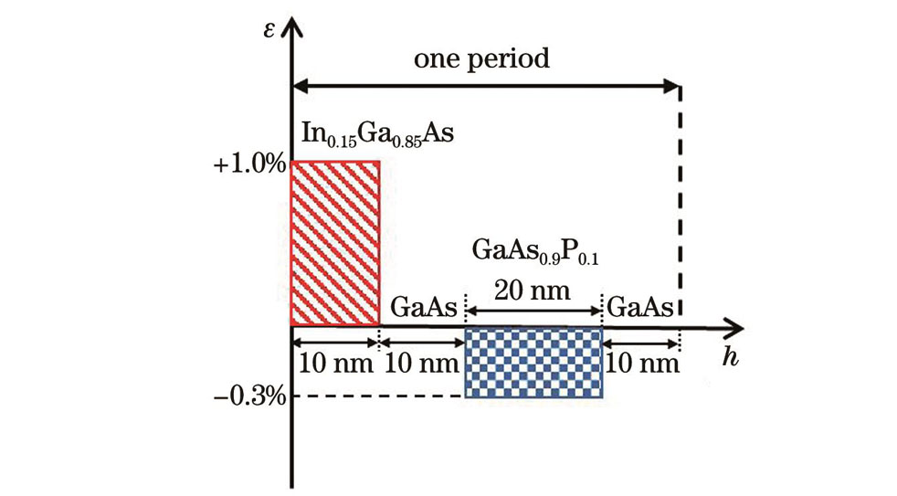
    Fig. 1. Schematic diagram of material, strain and thickness of each period of periodic superlattice
    Schematic diagram of material and structure of strain balanced superlattice
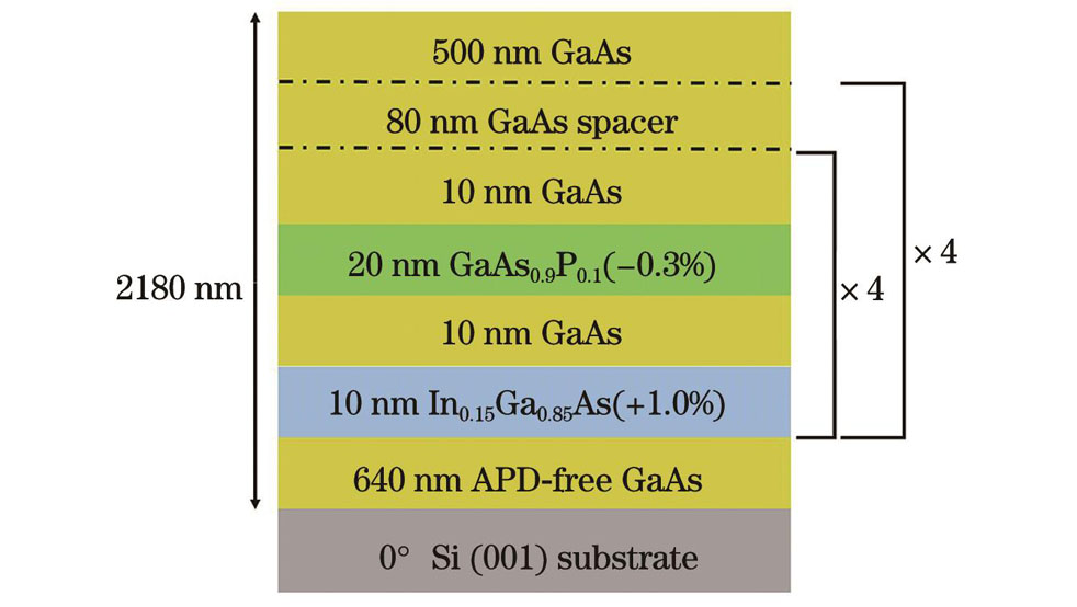
    Fig. 2. Schematic diagram of material and structure of strain balanced superlattice
    Measured surface toughness of samples A and B ( measurement range is 10 μm×10 μm). (a)-(e) Sample A; (f)-(j) sample B
    Fig. 3. Measured surface toughness of samples A and B ( measurement range is 10 μm×10 μm). (a)-(e) Sample A; (f)-(j) sample B
    Schematic diagrams of growth modes and surface morphology characteristic of samples A and B. (a) Schematic diagram of step flow growth mode; (b) schematic diagram of FM growth mode; (c) surface morphology characterization of sample A (1 μm×1 μm); (d) surface morphology characterization of sample B (1 μm×1 μm)
    Fig. 4. Schematic diagrams of growth modes and surface morphology characteristic of samples A and B. (a) Schematic diagram of step flow growth mode; (b) schematic diagram of FM growth mode; (c) surface morphology characterization of sample A (1 μm×1 μm); (d) surface morphology characterization of sample B (1 μm×1 μm)
    Comparison of PL curves of GaAs epitaxial layer of samples A and B. (a) Center; (b) right; (c) lower; (d) left; (e) upper
    Fig. 5. Comparison of PL curves of GaAs epitaxial layer of samples A and B. (a) Center; (b) right; (c) lower; (d) left; (e) upper
    XRD characterization curves of GaAs epitaxial layer of samples A and B
    Fig. 6. XRD characterization curves of GaAs epitaxial layer of samples A and B
    SampleRoot-mean-square(RMS)of surface toughness of different locations /nmAverage of RMS /nmStandard deviation of RMS
    CenterUpperRightLowerLeft
    A1.161.011.520.931.201.160.22
    B1.811.361.692.022.731.920.51
    Table 1. Surface toughness of samples A and B
    LocationPL intensityFWHM /nm
    Sample ASample BSample ASample B
    Average40378672623.431.6
    Center46200706323.231.3
    Upper48539454222.731.5
    Right46745233322.931.3
    Lower319611537823.932.5
    Left28443431624.331.3
    Table 2. PL intensity, FWHM and their mean value of samples A and B
    Jiachen Li, Jun Wang, Chunyang Xiao, Haijing Wang, Yanxing Jia, Zhuoliang Liu, Bojie Ma, Rui Ming, Qing Ge, Hao Zhai, Feng Lin, Weiyu He, Yongqing Huang, Xiaomin Ren. Investigation of Surface Improvement of GaAs/Si(001) with Strain Balanced Superlattice[J]. Chinese Journal of Lasers, 2023, 50(6): 0603002
    Download Citation