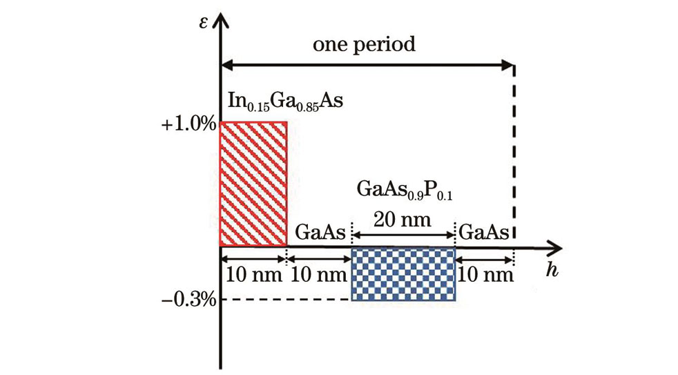
To realize a silicon-based photonic integrated chip circuit, we perform epitaxial deposition of GaAs material on a silicon substrate and subsequently prepare a silicon-based light source. However, there is a 4.1% lattice mismatch between Si and GaAs, resulting in three-dimensional (3D) growth of the material and formation of several 3D island structures in the initial growth stage of GaAs/Si (001), deteriorating its surface morphology. The roughness in the initial growth stage is difficult to reduce to an ideal level, which significantly affects the crystal quality of subsequent growth materials and leads to the failure of the overall preparation process of the device. Currently, the main solutions for reducing the surface roughness of GaAs/Si(001) materials are chemical mechanical polishing (CMP) and the growth of strained-layer superlattice (SLS). Because the epitaxial layer is too thin to be cleaned using the CMP technology, the possibility of polishing the epitaxial layer cannot be increased because of the complexity of epitaxial layer preparation. Therefore, the SLS growth technology has become the primary choice for improving the surface morphology of epitaxial materials. Generally, the SLS growth technology used in previous study matches the lattice of epitaxial materials, and its strain is significantly less than that of the SLS used as a dislocation filter layer. Therefore, it can only improve the surface morphology; however, it cannot reduce the material defects and improve the crystal quality. Therefore, it is necessary to use a dislocation filter layer to improve the crystal quality of GaAs/Si (001). In this study, the preparation technology of a strain-balanced superlattice structure that combines tensile and compressive strains is proposed. This technique can not only effectively improve the surface roughness of GaAs/Si (001) materials but also reduce material defects and enhance the crystal quality in the traditional dislocation filter layer. This not only simplifies the growth and preparation process of GaAs/Si (001) but also reduces the thickness of the epitaxial layer, thereby reducing the risk of thermal cracking caused by excessive material thickness.
GaAs epitaxial layers with strain-balanced superlattices were grown through metal organic chemical vapor deposition on exact planar silicon (001), and pure GaAs epitaxial layers were grown under the same conditions. The surface morphology and crystal quality of the two samples were characterized by atomic force microscopy (AFM), photoluminescence (PL), and double crystal X-ray diffraction (XRD).
The implementation of the strain-balanced superlattice technique changes the growth mode of the GaAs/Si(001) material from layer-by-layer growth to step-flow growth. As demonstrated in the AFM characterization, the average surface root mean square (RMS) roughness decreases from 1.92 nm (10 μm×10 μm) to 1.16 nm (10 μm×10 μm) (Fig. 3 and Table 1). The quality of the GaAs crystals is characterized by PL and XRD at room temperature. In comparison with the GaAs/Si(001) material without a superlattice, the PL peak intensity of the GaAs/Si(001) material with a superlattice increases by 500.3%, whereas the average PL peak full width at half maximum (FWHM) reduces from 31.6 nm to 23.4 nm (Fig. 5 and Table 2). The FWHM of the XRD curve decreases by 30.4%, whereas its peak intensity increases by 472.2% (Fig. 6).
In this study, the effects of strain-balanced superlattice on the surface morphology and crystal quality of GaAs/Si(001) are experimentally investigated. The results indicate that this scheme can effectively improve the surface morphology of GaAs/Si(001). Compared with the GaAs epitaxial layer without the application of this technique, the average RMS roughness of the prepared sample decreases from 1.92 nm (10 μm×10 μm) to 1.16 nm (10 μm×10 μm). In terms of crystal quality, compared with GaAs epitaxial layer prepared without this technique, the average PL peak intensity under room temperature characterization increases by 500.3%, whereas the average PL peak FWHM decreases from 31.6 nm to 23.4 nm. The FWHM of the XRD curve decreases by 30.4%, whereas its peak intensity increases by 472.2%. In conclusion, this scheme effectively improves the surface morphology and crystal quality of GaAs/Si(001) materials. The scheme proposed in this paper provides a feasible way to improve the surface morphology of silicon-based GaAs materials and lays a technical foundation for promoting the industrialization of large-scale silicon-based photoelectric integrated circuits.