
Yuexin YIN, Xinru XU, Yingzhi DING, Mengke YAO, Guoyan ZENG, Daming ZHANG. Progress and Challenge of 3D Photonic Integrated Circuit(Invited)[J]. Acta Photonica Sinica, 2022, 51(7): 0751416
- Acta Photonica Sinica
- Vol. 51, Issue 7, 0751416 (2022)
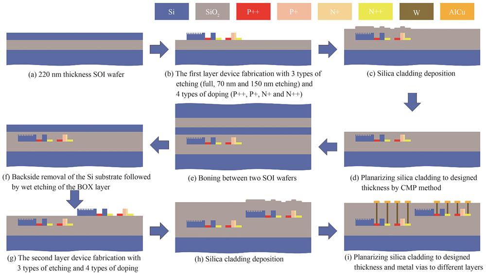
Fig. 1. Overview of bonding fabrication for 3D PIC on SiPh
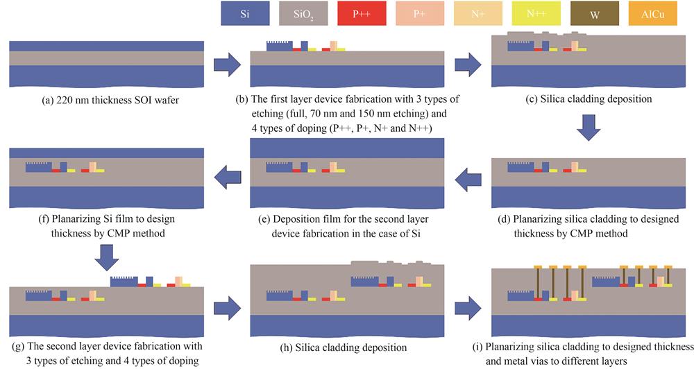
Fig. 2. Overview of deposition fabrication for 3D PIC on SiPh
Fig. 3. SEM image of microring resonator on the DLSOI platform[22]
Fig. 4. Overview of the 3-D heterogeneous integration platform used to construct the single-chip OPA[23]
Fig. 5. Grating based interlayer transition [24]
Fig. 6. Cross section SEM of polysilicon racetrack resonators coupled to crystalline silicon waveguides before oxide cladding. Inset shows the definition of r and coupling length L0[27]
Fig. 7. Raman spectra and SEM micrographs of poly-Si waveguide after laser crystallized[30]
Fig. 8. Schematic of multilayer platform including tapered vertical coupler and waveguides crossing[36]
Fig. 9. Fabricated multilayer star-coupler and its test results[36]
Fig. 10. Schematic of the proposed three layer SiN-on-Si platform and its X-TEM images[37]
Fig. 11. Optical micrograph of a fabricated S&S 4 × 4 switch[38]
Fig. 12. Circuit diagram,microscopic image and the measured losses of the proposed polarization-diversity PILOSS switch[39]
Fig. 13. 3D integrated wavelength demultiplexer[47]
Fig. 14. 2D OPAs based on PolyBoard PICs [48]
Fig. 15. 3D six-mode(de)multiplexer[51]
|
Table 1. Progress of 3D photonics integrated circuits


Set citation alerts for the article
Please enter your email address

© Copyright 2018-2021 | Chinese Laser Press. All Rights Reserved 沪ICP备15018463号-20