• Acta Photonica Sinica
  • Vol. 51, Issue 7, 0751416 (2022)
Yuexin YIN, Xinru XU, Yingzhi DING, Mengke YAO, Guoyan ZENG, and Daming ZHANG*
Author Affiliations
  • State Key Laboratory of Integrated Optoelectronics,College of Electronic Science and Engineering,Jilin University,Changchun 130012,China
  • show less
    DOI: 10.3788/gzxb20225107.0751416 Cite this Article
    Yuexin YIN, Xinru XU, Yingzhi DING, Mengke YAO, Guoyan ZENG, Daming ZHANG. Progress and Challenge of 3D Photonic Integrated Circuit(Invited)[J]. Acta Photonica Sinica, 2022, 51(7): 0751416 Copy Citation Text show less

    Abstract

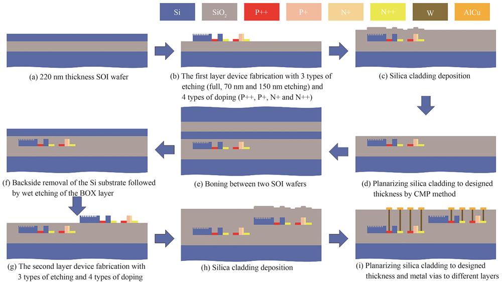
    The ever-increasing demand for high bandwidth is continued to grow in the forthcoming era of the Internet of Things (IoT) and 5G. Photonic Integrated Circuit (PIC), especially Silicon Photonics (SiPh), compatible with Complementary Metal-Oxide-Semiconductor (CMOS) technologies, is a solution for a high capacity and low power consumption communication. However, the scale of PIC is limited by optical loss and reticle size of Ultraviolet (UV) lithography, which is far from meeting the requirements of high-speed data communication and networking in Data Centers (DCs) and High Performance Computers (HPCs). Three dimensional integration Photonic Integrated Circuits (3D PICs), like the 3D integrated electronics, overcome many limitations of 2D photonic devices where all photonic components are on the same plane. Till now, several 3D PICs have been designed, proposed and experimentally demonstrated on different materials platforms, including SOI, SiN-on-SOI and polymer platforms. Wafer bonding and low temperature deposition are two general methods to fabricate 3D PICs. Wafer bonding is an effective way to achieve multilayer SOI devices for 3D PICs and photonic electronic integrated circuits. Also, bonding offers a method for 3D heterogeneous integration between Ⅲ-Ⅴ on silicon, which is an on-chip source solution. However, the cost of bonding equipment and fabrication is too expensive. Besides, several materials, including silicon nitride (SiN), amorphous silicon (a-Si) and polycrystalline silicon (poly-Si), have been deposited on SOI wafer to conduct 3D PICs. Although SiN has some unique advantages, such as extremely low propagation loss, the large fabrication tolerance, SiN itself has no active effect (low thermal tuning). Therefore, SiN-on-SOI platform has been provided by many CMOS pilot lines, leveraging on both advantages of Si and SiN platform. However, multi active layers are still required in many applications such as optical switch and Optical Phase Array (OPA). A-Si is a similar material like SiN. And A-Si is possible turned to poly-Si with an order higher mobility by high temperature annealing or laser crystallizing. Laser crystallizing is a potential method for low loss and high mobility poly-Si, but lots of efforts are still needed to achieve wafer scale fabrication. Benefiting from low cost and simple fabrication, several optical devices have been experimentally demonstrated on polymer-based Planar Lightwave Circuits (PLCs) platform. The low index difference between the cores and cladding leads the core size of polymer to several micrometers, which is hard to achieve high dense PICs. The 3D integration polymer PLC could improve the integration degree effectively, and lots of 3D polymer-based devices have been proposed, including wavelength division multiplexer/demutiplexers, mode division multiplexer/demutiplexers and OPAs.In summary, to develop 3D devices, this study widely researched the design, fabrication method and measurement methods. Till now, several 3D devices based on different materials platforms have been carefully analyzed and demonstrated experimentally. In this review, we overview the origin, development, recent progress of 3D PICs along with the applications of these devices. In our opinion, the 3D integration offers a platform not only a denser integration but also a multi-functional or multi-materials integration platform, which contains sources, modulators, optical routers, photodetectors and their drivers on one chip.
    Yuexin YIN, Xinru XU, Yingzhi DING, Mengke YAO, Guoyan ZENG, Daming ZHANG. Progress and Challenge of 3D Photonic Integrated Circuit(Invited)[J]. Acta Photonica Sinica, 2022, 51(7): 0751416
    Download Citation