
Carolien Castenmiller, Harold J. W. Zandvliet. On the mystery of the absence of a spin-orbit gap in scanning tunneling microscopy spectra of germanene[J]. Journal of Semiconductors, 2020, 41(8): 082003
- Journal of Semiconductors
- Vol. 41, Issue 8, 082003 (2020)
Abstract
1. Introduction
Since the rise of graphene[
![]()
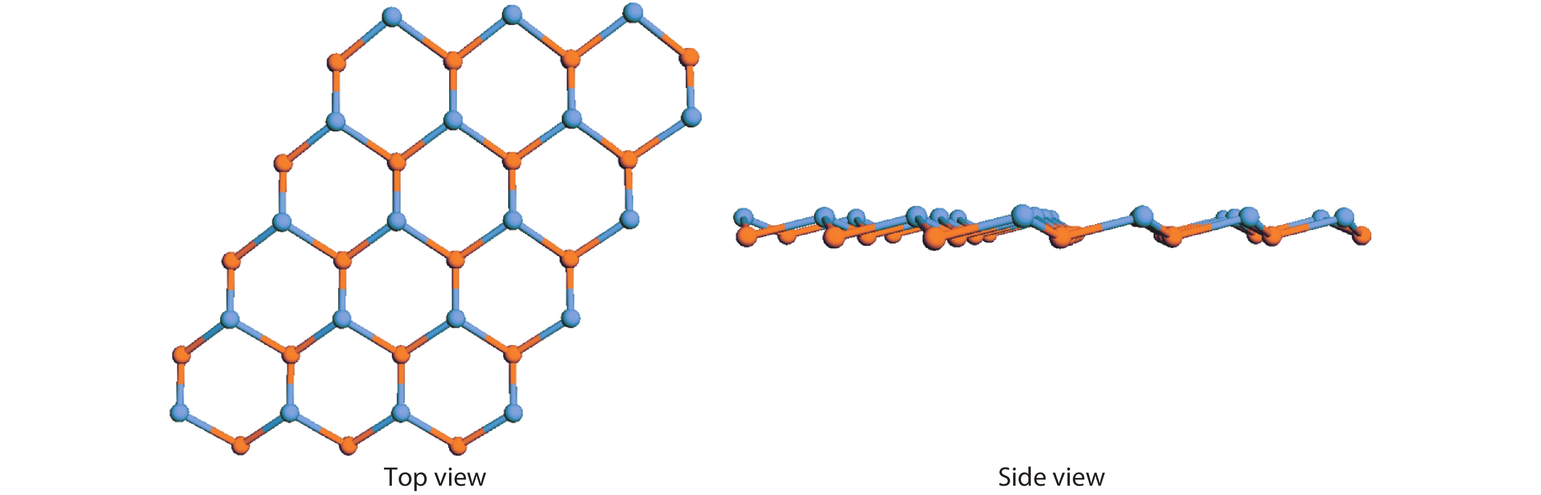
Figure 1.(Color online) Buckled honeycomb lattice of germanene.
Carbon occurs in nature in two allotropes: diamond and graphite. The diamond structure consists of sp3 hybridized carbon atoms, whereas the carbon atoms in the graphite structure are sp2 hybridized. At room temperature and atmospheric pressure the graphite structure has a lower energy than the diamond structure, which implies that diamonds are not forever. Unfortunately, diamond will eventually convert to graphite. In the case of silicon and germanium, however, this situation is reversed, i.e. the diamond structure is lower in energy than the layered graphite structure. Synthesizing or growing a single layer of silicene or germanene seems therefore, at least at first sight, a mission impossible. Fortunately, a single layer of sp3 hybridized silicon or germanium turns out to be instable. Cahangirov et al.[
In 2005 Kane and Mele[
In this paper we will scrutinize all the available scanning tunneling spectroscopy measurements that have been performed on germanene. We will elaborate on the effect that an electric field in the scanning tunneling microscopy junction can have on the size of the spin-orbit gap. We will show that the key to the absence of a spin-orbit gap in scanning tunneling spectra is the low work function of germanene. Germanene has a work function of only 3.8 eV[
2. Results and discussion
In the literature there are three germanene systems for which scanning tunneling spectroscopy experiments are performed. We will discuss these three examples one-by-one and in chronological order. The first system is germanene synthesized on Ge2Pt clusters[
As we will argue below the origin for the absence or strongly suppressed spin-orbit gap of germanene in scanning tunneling spectroscopy is caused by the electric field,
where ζ = ± 1 refers to the K (K’ ) point, s = ± 1 to the spin, Δ to the buckling of germanene, e to the unit of elementary charge,
![]()
Figure 2.(Color online) Schematic diagram of the band structure of germanene near the
3. Conclusions
The mystery regarding the absence of a spin-orbit gap in scanning tunneling spectroscopy measurements of germanene has been solved. We found that scanning tunneling spectroscopy is not the ideal technique to probe the spin-orbit gap and the quantum spin Hall effect in germanene owing to its very low work function of only 3.8 eV and buckled honeycomb structure. The difference in work function between germanene and scanning tunneling microscopy tip (for instance 4.5 eV for W and 5.5 eV for Pt/Ir) results in a substantial electric field of the order of 1 eV/nm that has a dramatic effect on the measured size of the spin-orbit gap of germanene. We anticipate that our findings are also relevant for other two-dimensional Dirac materials that have a buckled honeycomb structure.
Acknowledgements
CC and HJWZ acknowledge the Nederlandse Organisatie voor Wetenschappelijk Onderzoek (NWO) for financial support.
References
[1] K S Novoselov, A K Geim, S V Morozov et al. Electric field effect in atomically thin carbon films. Science, 306, 666(2004).
[2] A K Geim, K S Novoselov. The rise of graphene. Nat Mater, 6, 183(2007).
[3] K Takeda, K Shiraishi. Theoretical possibility of stage corrugation in Si and Ge analogs of graphite. Phys Rev B, 50, 14916(1994).
[4] P Vogt, P de Padova, C Quaresima et al. Silicene: compelling experimental evidence for graphenelike two-dimensional silicon. Phys Rev Lett, 108, 155501(2012).
[5] P Bampoulis, L Zhang, A Safaei et al. Germanene termination of Ge2Pt crystals on Ge(110). J Phys Condens Matter, 26, 442001(2014).
[6] F F Zhu, W J Chen, Y Xu et al. Epitaxial growth of two-dimensional stanene. Nat Mater, 14, 1020(2015).
[7] S Cahangirov, M Topsakal, E Aktürk et al. Two- and one-dimensional honeycomb structures of silicon and germanium. Phys Rev Lett, 102, 236804(2009).
[8] A Acun, L Zhang, P Bampoulis et al. Germanene: the germanium analogue of graphene. J Phys Condens Matter, 27, 443002(2015).
[9] C L Kane, E J Mele. Z2 topological order and the quantum spin Hall effect. Phys Rev Lett, 95, 146802(2005).
[10] C L Kane, E J Mele. Quantum spin Hall effect in graphene. Phys Rev Lett, 95, 226801(2005).
[11] C C Liu, W X Feng, Y G Yao. Quantum spin Hall effect in silicene and two-dimensional germanium. Phys Rev Lett, 107, 076802(2011).
[12] B Borca, C Castenmiller, M Tsvetanova et al. Image potential states of germanene. 2D Mater, 7, 035021(2020).
[13] R van Bremen, P Bampoulis, J Aprojanz et al. Ge2Pt hut clusters: A substrate for germanene. J Appl Phys, 124, 125301(2018).
[14] L Zhang, P Bampoulis, A van Houselt et al. Two-dimensional Dirac signature of germanene. Appl Phys Lett, 107, 111605(2015).
[15] C J Walhout, A Acun, L Zhang et al. Scanning tunneling spectroscopy study of the Dirac spectrum of germanene. J Phys Condens Matter, 28, 284006(2016).
[16] L Zhang, P Bampoulis, A Rudenko et al. Structural and electronic properties of germanene on MoS2. Phys Rev Lett, 116, 256804(2016).
[17] Z H Qin, J B Pan, S Z Lu et al. Direct evidence of Dirac signature in bilayer germanene Islands on Cu(111). Adv Mater, 29, 1606046(2017).
[18] M Ezawa. A topological insulator and helical zero mode in silicene under an inhomogeneous electric field. New J Phys, 14, 033003(2012).
[19] C C Liu, H Jiang, Y G Yao. Low-energy effective Hamiltonian involving spin-orbit coupling in silicene and two-dimensional germanium and tin. Phys Rev B, 84, 195430(2011).

Set citation alerts for the article
Please enter your email address
© Copyright 2018-2021 | Chinese Laser Press. All Rights Reserved 沪ICP备15018463号-20