Author Affiliations
1Nanjing University, College of Engineering and Applied Sciences, National Laboratory of Solid State Microstructures, Key Laboratory of Intelligent Optical Sensing and Integration, Jiangsu Key Laboratory of Artificial Functional Materials, Nanjing, China2Collaborative Innovation Center of Advanced Microstructures, Nanjing, China3Nanjing University, School of Electronic Science and Engineering, Nanjing, Chinashow less
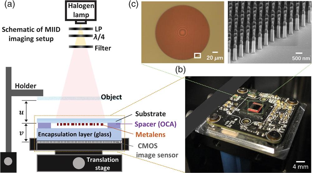
Fig. 1. Device architecture and metalens fabrication. (a) Schematic of the optical setup for MIID. (b) Photograph of the highly compact MIID. (c) Top-view optical microscope image and side-view SEM image of the fabricated -Si metalens with a diameter of .
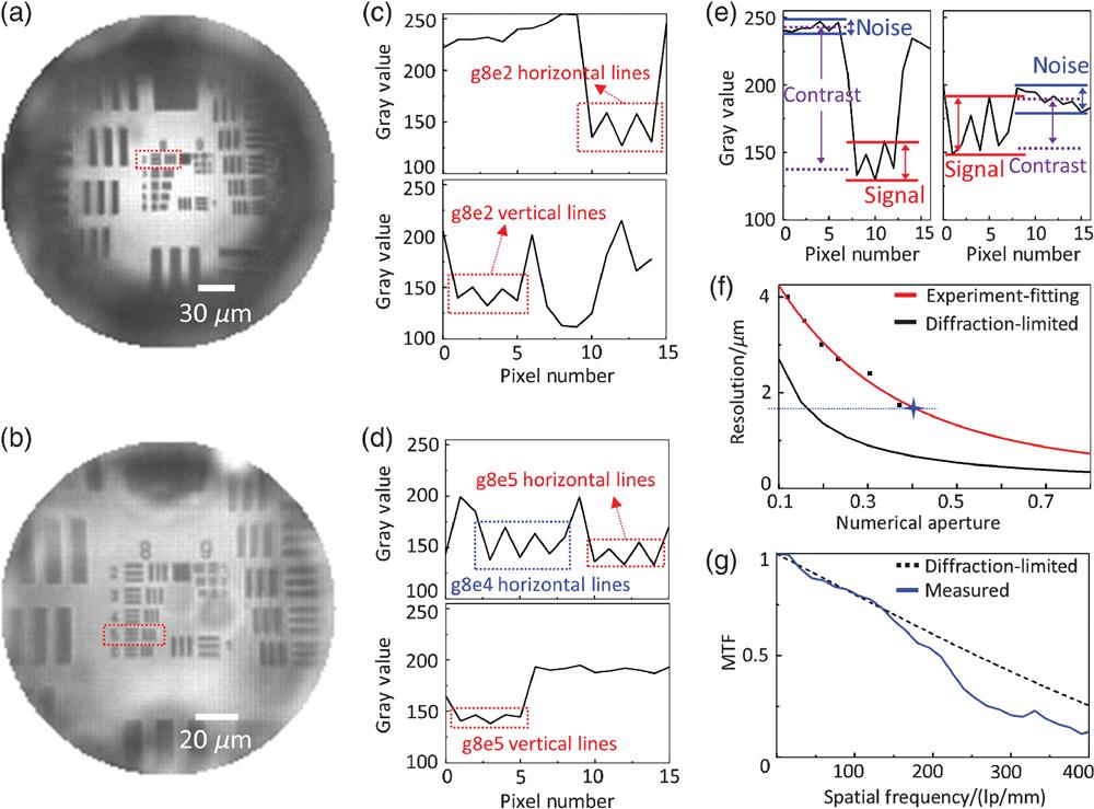
Fig. 2. Experimental characterization of a single -Si metalens on MIID. (a) Image of 1951 USAF resolution test chart taken from MIID with the metalens of at imaging distance of . (b) Image of 1951 USAF resolution test chart taken from MIID with the metalens of with image magnification. (c) Intensity distribution of horizontal lines and vertical lines of element 2, group 8 in the resolution test chart taken from the red dotted box in (a). (d) Intensity distribution of horizontal lines and vertical lines of element 5, group 8 in the resolution test chart taken from the red dotted box in (b). (e) Schematic diagram of signal, noise, and image contrast. Intensity distribution of horizontal lines of element 1, group 8 in (a) (left panel) and vertical lines of element 3, group 8 in (b) (right panel). (f) Resolution of metalenses with different NAs on MIID. The red line is the fitting curve from the experiment data plotted as black points, and the blue star denotes the pixel size of the CMOS image sensor. The black line is the resolution determined by the diffraction limit. (g) The measured MTF of MIID plotted with the theoretical diffraction-limited MTF.
Fig. 3. Spectral zooming of MIID. (a) Image of the 1951 USAF resolution test chart (group 6) taken from MIID at wavelengths of 560, 580, 600, 610, 620, and 630 nm. The whole image denotes the area of the metalens, and the blue dashed circle denotes the image area. (b) Optical image of double-side sample of characters DSL and NJU on top of and underneath the coverslip. . (c) Images of the double-side object captured by MIID at different wavelengths, where clear NJU is obtained at and DSL is obtained at .
Fig. 4. Imaging of MIID integrated with PMDP metalens array. (a) Phase distribution of PMDP metalens in the plane. The blue and red squares denote the phase distribution for LCP and RCP metalens regions, respectively. The corresponding dashed boxes demonstrate the limited FOV. (b) Optical microscope image of a PMDP metalens with size of . (c) Photograph of the fabricated PMDP metalens array. (d) Photograph of the prototype of MIID (sized about ). (e) Raw images of the USAF 1951 resolution chart by MIID with LCP (left panel) and RCP (right panel) illuminations. (f) Stitched image from sub-images of (e) through a certain image processing, as provided in Sec. S6 of the Supplementary Material. (g) Zoomed-in image to show the resolution.
Fig. 5. Conventional optical microscope (left) and MIID stitched images (right) of (a) Pap smear and (b) dragonfly wing. The optical microscope images are obtained with Olympus, , .