Abstract
Metasurfaces have demonstrated unprecedented capabilities in manipulating light with ultrathin and flat architectures. Although great progress has been made in the metasurface designs and function demonstrations, most metalenses still only work as a substitution of conventional lenses in optical settings, whose integration advantage is rarely manifested. We propose a highly integrated imaging device with silicon metalenses directly mounted on a complementary metal oxide semiconductor image sensor, whose working distance is in hundreds of micrometers. The imaging performances including resolution, signal-to-noise ratio, and field of view (FOV) are investigated. Moreover, we develop a metalens array with polarization-multiplexed dual-phase design for a wide-field microscopic imaging. This approach remarkably expands the FOV without reducing the resolution, which promises a non-limited space-bandwidth product imaging for wide-field microscopy. As a result, we demonstrate a centimeter-scale prototype for microscopic imaging, showing uniqueness of meta-design for compact integration.
1 Introduction
Current imaging technology has been well developed by versatile strategies for outstanding performances in high resolution, high image quality, and broad wavelength band. Most of these techniques are established on the basis of mature refractive or reflective optical elements, such as lenses, internal reflection mirrors, etc., which result in optical systems that are bulky, heavy, and inconvenient for portability. However, more compact, light, and stable optical systems are the ever-growing requirement of modern applications. Recent advances in computational imaging (including the lensless and scattering medium imaging) have shown a successful route to reduce the complexity of the optical system by discarding the refractive lenses.1,2 Nevertheless, they are not a real physical image, and the image quality strongly relies on the post-processing algorithms, such as iterative phase recovery algorithm,3,4 compressive sensing,5,6 and Fourier ptychography.7,8 It inevitably requires computational resources that are time consuming and sometimes needs particular prior knowledge for imaging reconstruction.
Benefiting from the development of nanofabrication technology, the metasurface as a new breakthrough of optical design has demonstrated tremendous capabilities in manipulating light by subwavelength unit cells,9–12 and fascinating applications with the low loss dielectric metasurfaces have been revealed.13–16 Among these applications, the metalens is one of the most promising candidates for upgrading current optical systems. During the past several years, exciting progress concerning the imaging performance of the metalens has been made, including improved efficiency,17,18 broadband achromaticism,19–21 broadened field-of-view (FOV),22,23 polarization functionalities,24,25 etc., which indicates a closer step toward real applications. As we revisit metasurface design besides those achievements, the ultrathin, ultralight, and flat architecture features as the core advantage of this newly developing optical design. However, only a few works focus on compact integration,26,27 and there is a lack of systematic characterization of imaging performance. In most previous works, metalenses act only as substitutes for conventional refractive lenses and play almost the same role in conventional optical settings without showing their uniqueness for integration.21,28–30
In this work, we directly integrate the metalenses onto the complementary metal oxide semiconductor (CMOS) image sensor to show the major advantage of the flat metalens. The metalenses were manufactured in amorphous silicon (-Si) nano-posts designed by the geometric Pancharatnam–Berry (PB) phase on a substrate, where the Si material was used for potential compatibility to full CMOS-based devices. After careful characterization of the imaging qualities with respect to the resolution, signal-to-noise ratio (SNR), FOV, and so on, we show the capability of this metalens-integrated imaging device (MIID) for spectral focal tuning31 due to the large dispersion. It breaks the limitation of lens-free shadow imaging that cannot resolve the depth-of-field (DOF) of the object.32 More importantly, we develop a metalens array to cover a wide area of CMOS image sensors for a wide-field imaging. To eliminate the blind areas in multiple-images-stitching, here, we utilize a polarization-multiplexed dual-phase (PMDP) design (with respect to two circular polarizations) to access two sets of lenses with complementary image areas. A full stitched wide-field image is completed only by switching the polarization without any mechanical movement. As a result, we achieved high-resolution images ( almost limited by image sensor pixel) with a millimeter-scale image area (expandable to whole centimeter-scale CMOS sensor), which was ultimately implemented in a size device prototype. This ultra-compact microscope system promises more exciting applications of metalens in high resolution, large FOV, and tunable DOF imaging.
Sign up for Advanced Photonics TOC. Get the latest issue of Advanced Photonics delivered right to you!Sign up now
2 Device Architecture and Fabrication
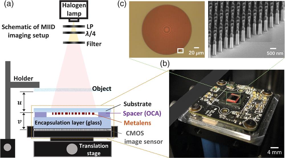
Figure 1(a) shows the schematics of imaging setup for our MIID. An optically clear adhesive (OCA) tape (Tesa, 69402) is used to transfer and fix the metalens on the CMOS image sensor (Imaging source, DMM 27UJ003-ML, pixel size: ) with proper thickness for imaging distance (the distance between the CMOS image sensor and metalens) in our experiment. Here, the OCA is employed for its colorless transparency with high transmittance () in the visible and near-infrared ranges, which is widely used in optoelectronic devices. We also take OCA tape as the spacer medium of integration for the well-defined stationary thickness. The detailed metalens integration process is further described in Sec. S1 of the Supplementary Material. With skillful operation, the integration deviation is very small, and the distortion caused by lens tilting can be handled. Once the metalens is mounted on the CMOS image sensor, the imaging distance is fixed, and a clear image can be acquired by tuning the object distance (the distance between metalens and object) with the translation stage. Figure 1(b) shows the photograph of the highly compact MIID (here, ). It should be noted that, due to the complex medium layers in both image space and object space of the metalens, the parameters () here are effective ones containing the influence of the medium. We first measured the effective imaging distance and take it as constant in our theoretical design. A white-light source of a halogen lamp with color filters was employed for incoherent monochromatic illumination. The metalens is designed as an aplanatic lens to eliminate on-axis aberrations for the imaging scheme () with a phase profile of31where is the designed working wavelength, is the focal length, and is the radial coordinate. This required phase profile is imparted via the geometric phase (i.e., PB phase), which is widely used in metasurface design.31,33,34 Here, we choose -Si as our metalens material for its high refractive index (), relatively low loss at long wavelengths in the visible (), and particularly its compatibility to the CMOS platform. A -diameter metalens composed of nano-posts is fabricated in an 850-nm-thick -Si film deposited on a -thick fused silica substrate. The metalens is designed to work at a wavelength of 630 nm with (diameter , ). To avoid high-order diffractions, the rectangular nano-post units are designed with sizes of in a height of 850 nm (equal to thickness of deposited Si film) and arranged in a square lattice with period of 400 nm. The simulated polarization conversion rate (PCR) is as high as for the unit structure to guarantee high efficiency. The PCR is defined as , where and represent the complex transmission coefficients of cross-polarized and co-polarized light, respectively. The metalens is fabricated using standard electron-beam lithography and dry etching. The detailed fabrication process is described in Sec. S1 of the Supplementary Material. The optical microscope image and scanning electron microscope (SEM) image of the metalens are shown in Fig. 1(c), respectively.

Figure 1.Device architecture and metalens fabrication. (a) Schematic of the optical setup for MIID. (b) Photograph of the highly compact MIID. (c) Top-view optical microscope image and side-view SEM image of the fabricated -Si metalens with a diameter of .
3 Characterization of the Single Metalens Imaging
The 1951 United States Air Force (USAF) resolution test chart (Edmund, Positive 1951 USAF Hi-Resolution Target) is used as the imaging target. Figure 2(a) shows the image formed by MIID with a metalens of at imaging distance of with operating wavelength at 630 nm, revealing resolution of (element 2, group 8), as shown in Fig. 2(c). The resolution of MIID is limited by the pixel size of the CMOS image sensor () without image magnification. Figure 2(b) shows the image obtained with metalens of (, ) at imaging distance with operating wavelength of 630 nm. The resolution is (element 5, group 8), as shown in Fig. 2(d), with image magnification of about 1.5. By careful observation, in Figs. 2(c) and 2(d) we find that the contrast of gray value of vertical lines is much weaker, which makes them hardly resolvable. It is due to the inequivalent CMOS pixels in two dimensions. Strictly speaking, our device only reaches the resolution of g8e2 () and g8e5 () in the -dimension in equal-size () and magnification image cases, respectively.
Figure 2.Experimental characterization of a single -Si metalens on MIID. (a) Image of 1951 USAF resolution test chart taken from MIID with the metalens of at imaging distance of . (b) Image of 1951 USAF resolution test chart taken from MIID with the metalens of with image magnification. (c) Intensity distribution of horizontal lines and vertical lines of element 2, group 8 in the resolution test chart taken from the red dotted box in (a). (d) Intensity distribution of horizontal lines and vertical lines of element 5, group 8 in the resolution test chart taken from the red dotted box in (b). (e) Schematic diagram of signal, noise, and image contrast. Intensity distribution of horizontal lines of element 1, group 8 in (a) (left panel) and vertical lines of element 3, group 8 in (b) (right panel). (f) Resolution of metalenses with different NAs on MIID. The red line is the fitting curve from the experiment data plotted as black points, and the blue star denotes the pixel size of the CMOS image sensor. The black line is the resolution determined by the diffraction limit. (g) The measured MTF of MIID plotted with the theoretical diffraction-limited MTF.
To get a compact imaging device, we did not add polarization analyzers between the metalens and the CMOS image sensor due to the limited space. The calculated high PCR also ensures the focus and imaging efficiency. To analyze the experimental imaging performances, we define , where denotes the intensity of the signal that can be clearly resolved, such as element 1, group 8, and denotes the standard deviation of the background noise intensity. For instance, Fig. 2(e) depicts the imaging data of USAF elements well under the resolution to evaluate the signal and noise [see the lines of element 1, group 8 in Fig. 2(a) in the left panel and lines of element 3, group 8 in Fig. 2(b) in the right panel]. To obtain an SNR as accurate as possible, we calculate SNR from multiple sets of signals and noises [Fig. 2(e)] and compute their average value as the calculated SNR. According to our experimental data, we get the SNR of about 19.89 dB in Fig. 2(a), which decreases to 9.23 dB in the magnification case in Fig. 2(b). Moreover, the image quality of Fig. 2(a) appears much better than Fig. 2(b) due to the sharper image signals over the background, which is usually determined by the image contrast. Here, we define it as , where indicates the average minimum signal intensity, and indicates the average background intensity, as shown in Fig. 2(e). Then, we calculated the image contrasts for Figs. 2(a) and 2(b) with the data of 0.33 and 0.15, respectively, showing better imaging performance in contrast to the equal size image in the system.
To get a systematic characterization of the imaging resolution by this MIID, a series of metalenses with different NAs on MIID were characterized at the imaging scheme [see Fig. 2(f)]. The discrepancy between the measured resolution and theoretical value would possibly be due to the imperfection of metalens fabrication, the background noises, and pixel-size limited CMOS image sensor; more discussion is provided in Sec. S2 of the Supplementary Material. Moreover, the modulation transfer function (MTF) was obtained by the slanted-edge method, which shows good agreement with theoretical diffraction-limited MTF at low spatial frequency, as plotted in Fig. 2(g). The discrepancy between our measured MTF and the diffraction limit at high spatial frequency would also probably be attributed to the background noises and pixel-size-limited CMOS sensor as well.
Although the metalens mounted on CMOS image sensor leads to a fixed imaging distance, we can realize optical zoom easily by tuning the working wavelength according to the large dispersive metalens.31 Taking a designed metalens (focal length of at ) as an example, we obtained the images of USAF 1951 target (part of group 6) at , 580, 600, 610, 620, and 630 nm with an imaging distance as constant at about [see Fig. 3(a) where the area inside the blue dashed circle displays the image by MIID; more discussion in Sec. S3 of the Supplementary Material]. Due to the chromatic dispersion of the metalens, the focal length will be longer at shorter wavelengths, which results in a decreased NA and zoom-out imaging at a constant imaging distance. Inheriting the chromatic dispersion, this MIID is capable of acquiring the depth of objects without mechanical movement. To manifest this function, we fabricated two microscale samples on the top (side A) and bottom (side B) of a glass coverslip, as schematically shown in Fig. 3(b) (see imaging setup in Fig. S1 in the Supplementary Material). Here, characters “DSL” and “NJU” were fabricated on both sides of a coverslip by maskless lithography with a distance of (i.e., coverslip thickness). The whole lateral sizes of the two objects are both . With a certain image distance (), we illuminate the sample with light of different wavelengths. From Fig. 3(c), a clear image of NJU but a blurred DSL image is observed at , and vise versa at . It does demonstrate the capability of DOF tuning via switching the illumination wavelength.
Figure 3.Spectral zooming of MIID. (a) Image of the 1951 USAF resolution test chart (group 6) taken from MIID at wavelengths of 560, 580, 600, 610, 620, and 630 nm. The whole image denotes the area of the metalens, and the blue dashed circle denotes the image area. (b) Optical image of double-side sample of characters DSL and NJU on top of and underneath the coverslip. . (c) Images of the double-side object captured by MIID at different wavelengths, where clear NJU is obtained at and DSL is obtained at .
4 Wide-Field Imaging of MIID Integrated with PMDP Metalens Array
There have been several works dedicated to image aberration correction with singlet or doublet metalenses to enlarge the imaging FOV.26,27,35 However, an increase of the metalens size to a macroscopic size in the single axis imaging scheme will inevitably increase the working distance, which definitely weakens the ultrathin and ultralight advantages of metalenses. We prefer the MIID to work in a short-working distance in an enlarged FOV, to keep the advantage of compact integration as it is mounted to the CMOS image sensor. However, the imaging principle constrains the single lens size with very limited imaging area, which greatly prevents its practical application. To circumvent this limitation and obtain a large FOV imaging, we proposed a metalens array for MIID to acquire multiple images and stitch them together.30,36 Due to the small FOV of individual metalenses (see details in Sec. S4 of the Supplementary Material), only part of the object can be imaged, and these images will not overlap in a imaging system.37,38 Therefore, there will be blind areas as we stitch these sub-images, which prohibits constructing a complete image.
Fortunately, a powerful capability of the metasurface is the flexible design with multiplexed functions in a single device,39,40 which possibly provides a solution to make up the blind areas of the FOV. Recently, a general polarization multiplexed metasurface has been established via merging the geometric and propagation phases together to independently control phase profiles in two orthogonal polarization states, including the two circular polarization states.24,41–45 Here, in order to cover the blind area among limited FOV of our MIID in a single-shot imaging process, we proposed a PMDP metalens design with cross phase profiles of certain lens areas to satisfy the requirements of two different focusing lenses working at left-hand circular polarization (LCP) and right-hand circular polarization (RCP), respectively, as shown in Fig. 4(a) (more details about the design of PMDP metalenses are provided in Sec. S5 of the Supplementary Material). By simply switching polarization states, we can obtain two independent images.
Figure 4.Imaging of MIID integrated with PMDP metalens array. (a) Phase distribution of PMDP metalens in the plane. The blue and red squares denote the phase distribution for LCP and RCP metalens regions, respectively. The corresponding dashed boxes demonstrate the limited FOV. (b) Optical microscope image of a PMDP metalens with size of . (c) Photograph of the fabricated PMDP metalens array. (d) Photograph of the prototype of MIID (sized about ). (e) Raw images of the USAF 1951 resolution chart by MIID with LCP (left panel) and RCP (right panel) illuminations. (f) Stitched image from sub-images of (e) through a certain image processing, as provided in Sec. S6 of the Supplementary Material. (g) Zoomed-in image to show the resolution.
Figure 4(b) shows the optical microscopic image of a PMDP metalens with size of . We arranged the metalens into a array, containing metalens for LCP multiplexed with metalens for RCP. The entire lens region is about , as shown in Fig. 4(c). Each metalens is designed at an operating wavelength of 630 nm and focal length of . To demonstrate the advances in compact integration, we have packaged the whole imaging system into a significantly miniaturized prototype with a size about . Figure 4(d) shows a photograph of the prototype including the LED matrix, LED controller, polarizers, sample holder, and core component of MIID. The images of the resolution test chart for LCP and RCP incident light taken from MIID with the PMDP metalens array are shown in Fig. 4(e), respectively. The image distortion caused by monochromatic aberration is observable by the naked eye, especially for objects with large feature size. Figure 4(f) shows a stitched image by combining two sets of sub-images after distortion correction and background subtraction (the detailed proceeding is provided in Sec. S6 of the Supplementary Material). The stitched image demonstrated a wide FOV area, the same as the metalens array region () without losing the resolution [, element 2, group 8; see Fig. 4(g)]. The stitched image has some stitching artifacts such as diagonal stripes due to the uneven brightness at the center and edge of sub-images caused by vignetting. At present, the performances of our MIID are still lower than that of lensless imaging (e.g., Ref. 8) both in resolution and FOV; however, MIID provides a totally new route that holds development potential for high-speed large-FOV microscopy. Moreover, our imaging process is much simpler and timesaving (our processing time is on a laptop, while 50 s with a desktop computer is needed in Ref. 8) compared with those sophisticated post-processing algorithms in lensless imaging and would significantly save computing resources.
As an example for application, we used this MIID to image a biospecimen of a Pap smear and dragonfly wing (as shown in Fig. 5). Compared to the optical microscope images (Olympus, objective, ) in the left panels of Fig. 5, the stitched images show good consistency and better contrast for these translucent or low index-contrast biospecimens. This stitched image covers times the area of a single metalens without decreasing the resolution and increasing the working distance, which is ready to expand to much larger areas until it covers the whole CMOS image sensor. Therefore, our approach does provide a successful solution to break the restriction between high resolution and wide FOV and make it feasible for high-throughput bioimaging and diagnosis.
Figure 5.Conventional optical microscope (left) and MIID stitched images (right) of (a) Pap smear and (b) dragonfly wing. The optical microscope images are obtained with Olympus, , .
5 Discussions and Conclusion
We have shown a metalens-integrated compact imaging device for wide-field microscopy achieved by directly mounting the metalens to an image sensor. Based on the silicon metalens working in the red light wavelength range, the imaging performances of the integrated system, including the resolution, SNR, imaging aberration, and FOV, were systematically investigated. The spectral optical zooming and DOF-resolved imaging have been achieved by taking advantage of the large dispersion of the metalens. More importantly, the metalens array with polarization multiplexing is used to reach a wide FOV imaging, which breaks the link between resolution and FOV. Finally, a miniaturized prototype is demonstrated to show the powerful capability of compact integration. Frankly, the performance of the current MIID is not good enough compared with conventional microscope and some of the computational imaging devices. In addition to the stitching artifacts that can be further improved by optimization, the relatively low working efficiency of the metalens would mainly account for background noises and restricted imaging performance. Fortunately, there are still opportunities in improving the efficiency of metalenses by adopting low-loss materials (e.g., GaN and SiN) and higher aspect-ratio nano-post elements. Moreover, future development of smaller pixels of the CMOS sensor will also enhance the MIID capability for higher resolutions. Our approach provides a new solution of ultra-compact and wide-field imaging by taking advantage of metasurfaces, which may inspire more revolutionary compact optical devices.
References
[1] A. Ozcan, E. McLeod. Lensless imaging and sensing. Annu. Rev. Biomed. Eng., 18, 77-102(2016).
[2] N. Antipa et al. Diffusercam: lensless single-exposure 3D imaging. Optica, 5, 1-9(2018).
[3] J. Zhang et al. Adaptive pixel-super-resolved lensfree in-line digital holography for wide-field on-chip microscopy. Sci. Rep., 7, 11777(2017).
[4] A. Berdeu et al. Comparative study of fully three-dimensional reconstruction algorithms for lens-free microscopy. Appl. Opt., 56, 3939-3951(2017).
[5] G. Satat, M. Tancik, R. Raskar. Lensless imaging with compressive ultrafast sensing. IEEE Trans. Comput. Imaging, 3, 398-407(2017).
[6] T. Nakamura et al. Super field-of-view lensless camera by coded image sensors. Sensors, 19, 1329(2019).
[7] T. Aidukas et al. Low-cost, sub-micron resolution, wide-field computational microscopy using opensource hardware. Sci. Rep., 9, 7457(2019).
[8] S. Jiang et al. Wide-field, high-resolution lensless on-chip microscopy via near-field blind ptychographic modulation. Lab Chip, 20, 1058-1065(2020).
[9] N. Yu et al. Light propagation with phase discontinuities: generalized laws of reflection and refraction. Science, 334, 333-337(2011).
[10] D. Lin et al. Dielectric gradient metasurface optical elements. Science, 345, 298-302(2014).
[11] N. Yu, F. Capasso. Flat optics with designer metasurfaces. Nat. Mater., 13, 139-150(2014).
[12] A. Arbabi et al. Dielectric metasurfaces for complete control of phase and polarization with subwavelength spatial resolution and high transmission. Nat. Nanotechnol., 10, 937-943(2015).
[13] M. Faraji-Dana et al. Compact folded metasurface spectrometer. Nat. Commun., 9, 4196(2018).
[14] E. Nazemosadat et al. Dielectric broadband metasurfaces for fiber mode-multiplexed communications. Adv. Opt. Mater., 7, 1801679(2019).
[15] F. Yesilkoy et al. Ultrasensitive hyperspectral imaging and biodetection enabled by dielectric metasurfaces. Nat. Photonics, 13, 390-396(2019).
[16] F. Balli et al. A hybrid achromatic metalens. Nat. Commun., 11, 3892(2020).
[17] S. Byrnes et al. Designing large, high-efficiency, high-numerical-aperture, transmissive meta-lenses for visible light. Opt. Express, 24, 5110-5124(2018).
[18] T. Phan et al. High-efficiency, large-area, topology-optimized metasurfaces. Light Sci. Appl., 8, 48(2019).
[19] W. T. Chen et al. A broadband achromatic metalens for focusing and imaging in the visible. Nat. Nanotechnol., 13, 220-226(2018).
[20] S. Wang et al. A broadband achromatic metalens in the visible. Nat. Nanotechnol., 13, 227-232(2018).
[21] S. Shrestha et al. Broadband achromatic dielectric metalenses. Light Sci. Appl., 7, 85(2018).
[22] B. Groever, W. T. Chen, F. Capasso. Meta-lens doublet in the visible region. Nano Lett., 17, 4902-4907(2017).
[23] Y. Guo et al. High-efficiency and wide-angle beam steering based on catenary optical fields in ultrathin metalens. Adv. Opt. Mater., 6, 1800592(2018).
[24] J. P. B. Mueller et al. Metasurface polarization optics: independent phase control of arbitrary orthogonal states of polarization. Phys. Rev. Lett., 118, 113901(2017).
[25] N. A. Rubin et al. Matrix Fourier optics enables a compact full-Stokes polarization camera. Science, 365, eaax1839(2019).
[26] A. Arbabi et al. Miniature optical planar camera based on a wide-angle metasurface doublet corrected for monochromatic aberrations. Nat. Commun., 7, 13682(2016).
[27] Y. Zhou et al. Flat optics for image differentiation. Nat. Photonics, 14, 316-323(2020).
[28] M. Khorasaninejad et al. Metalenses at visible wavelengths: diffraction-limited focusing and subwavelength resolution imaging. Science, 352, 1190-1194(2016).
[29] Z.-B. Fan et al. Silicon nitride metalenses for close-to-one numerical aperture and wide-angle visible imaging. Phys. Rev. Appl., 10, 014005(2018).
[30] R. Lin et al. Achromatic metalens array for full-colour light-field imaging. Nat. Nanotechnol., 14, 227-231(2019).
[31] C. Chen et al. Spectral tomographic imaging with aplanatic metalens. Light Sci. Appl., 8, 99(2019).
[32] G. Jin et al. Lens-free shadow image based high-throughput continuous cell monitoring technique. Biosens. Bioelectron., 38, 126-131(2012).
[33] L. Huang et al. Dispersionless phase discontinuities for controlling light propagation. Nano Lett., 12, 5750-5755(2012).
[34] G. Zheng et al. Metasurface holograms reaching 80% efficiency. Nat. Nanotechnol., 10, 308-312(2015).
[35] J. Engelberg et al. Near-IR wide-field-of-view Huygens metalens for outdoor imaging applications. Nanophotonics, 9, 361-370(2020).
[36] J. M. Moghimi et al. Micro-Fresnel-zone-plate array on flexible substrate for large field-of-view and focus scanning. Sci. Rep., 5, 15861(2016).
[37] R. Ng et al. Light field photography with a hand-held plenoptic camera(2005).
[38] R. Prevedel et al. Simultaneous whole-animal 3D imaging of neuronal activity using light-field microscopy. Nat. Methods, 11, 727-730(2014).
[39] S. Boroviks et al. Multifunctional metamirror: polarization splitting and focusing. ACS Photonics, 5, 1648-1653(2017).
[40] L. Jin et al. Noninterleaved metasurface for (26−1) spin- and wavelength-encoded holograms. Nano Lett., 18, 8016-8024(2018). https://doi.org/10.1021/acs.nanolett.8b04246
[41] N. A. Rubin et al. Polarization state generation and measurement with a single metasurface. Opt. Express, 26, 21455-21478(2018).
[42] B. Groever et al. High-efficiency chiral meta-lens. Sci. Rep., 8, 7240(2018).
[43] A. C. Overvig et al. Dielectric metasurfaces for complete and independent control of the optical amplitude and phase. Light Sci. Appl., 8, 92(2019).
[44] P. Huo et al. Photonic spin-multiplexing metasurface for switchable spiral phase contrast imaging. Nano Lett., 20, 2791-2798(2020).
[45] R. Y. Tsai. A versatile camera calibration technique for high-accuracy 3D machine vision metrology using off-the-shelf TV camera and lenses. IEEE J. Rob. Autom., 3, 323-344(1987).