
Yuanshuai Lü, Chenggen Wang, Wei Yuan, Guiju Zhang, Kaiyue Qi. Reconfigurable Mode Multiplexer Waveguide Switch Based on Phase Change Material[J]. Acta Optica Sinica, 2021, 41(17): 1723001
- Acta Optica Sinica
- Vol. 41, Issue 17, 1723001 (2021)
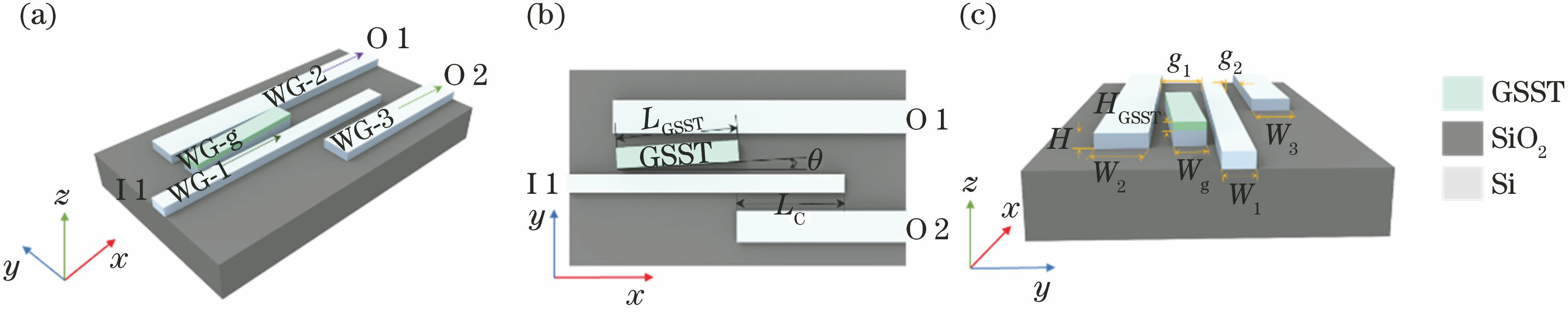
Fig. 1. 1×2 mode multiplexer switch. (a) Schematic of structure; (b) top view; (c) front view
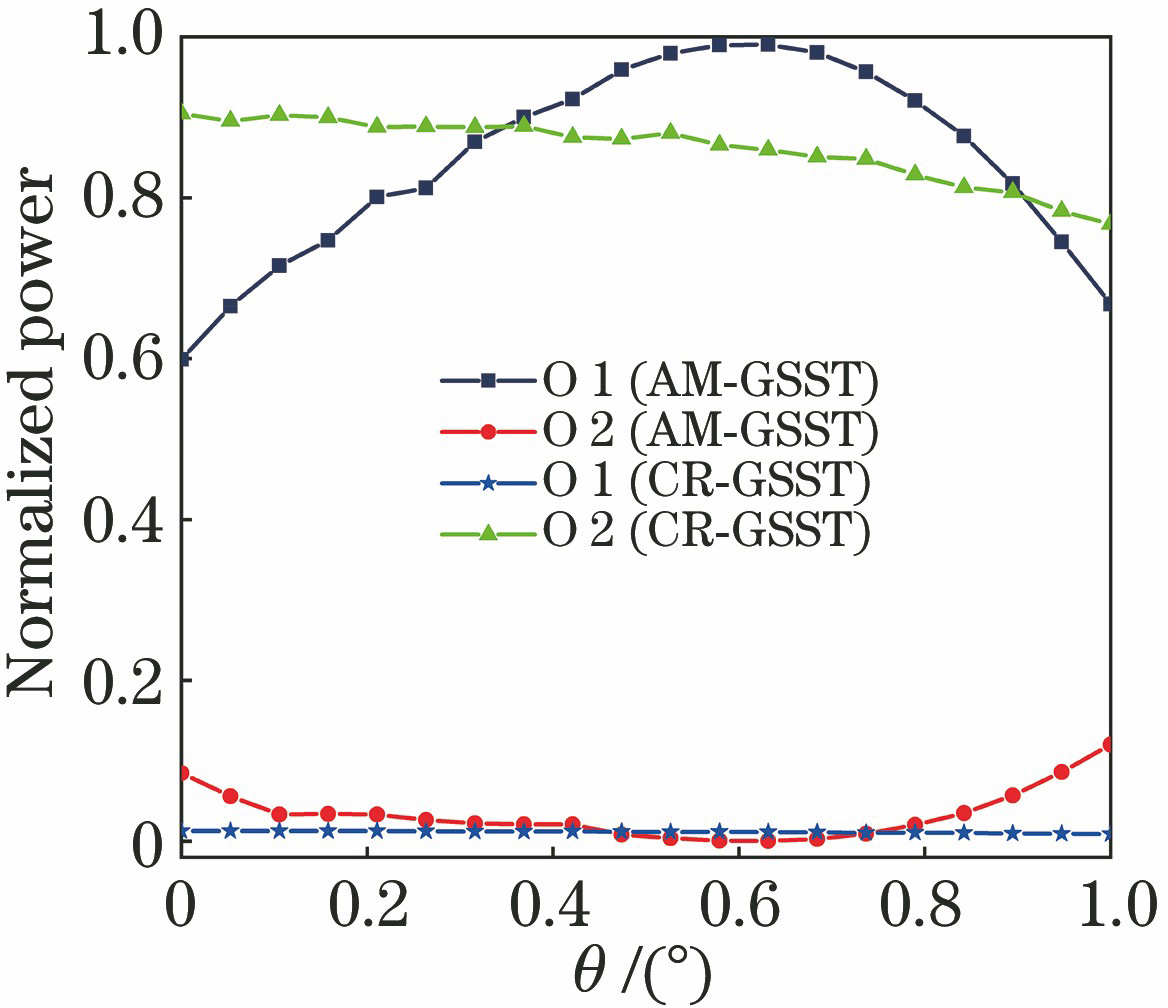
Fig. 2. Relationship between tilt angle of waveguide WG-g and normalized output power of 1×2 switch
Fig. 3. Relationship between wavelength and different parameters of GSST films in different phase states
Fig. 4. Performance curves and mode field distribution of silicon waveguide. (a) Relationship between effective refractive index and width of silicon waveguide; (b) mode field distribution of TM0 mode; (c) mode field distribution of TM1 mode
Fig. 5. Performance curve and mode field distribution of composite waveguide. (a) Relationship between effective refractive index of TM0 mode and thickness of GSST film; (b) mode field distribution of TM0 mode
Fig. 6. Optical field intensity distribution of supermode in directional waveguide couplers. (a) Optical field intensity distribution of even supermode; (b) optical field intensity distribution of odd supermode
Fig. 7. 2×2 multiplexer switch. (a) Top view; (b) cross-section of coupling region
Fig. 8. Optical field intensity distribution of supermode in triple directional waveguide couplers. (a) Optical field intensity distribution of TM0-A supermode; (b) optical field intensity distribution of TM0-B supermode; (c) optical field intensity distribution of TM0-C supermode
Fig. 9. Dispersion curves of different supermodes in triple waveguide. (a) Variation curves of effective index with width of composite waveguide; (b) variation curve of normalized power with length of composite waveguide
Fig. 10. Reconfigurable 2×4 mode multiplexer switch. (a) Schematic of structure; (b) top view
Fig. 11. Simulation results of each port of 1×2 mode multiplexer switch. (a) Optical field intensity distribution for amorphous GSST; (b) optical field intensity distribution for crystalline GSST
Fig. 12. Simulation results of each port of 2×2 mode multiplexer switch. (a) Optical field intensity distribution for amorphous GSST; (b) optical field intensity distribution for crystalline GSST
Fig. 13. Simulation output of optical field intensity of each port of 2×4 optical waveguide multiplexing switch under different states of GSST film. (a) I 1-O 1; (b) I 1-O 2; (c) I 1- O 3; (d) I 1-O 4; (e) I 2-O 1; (f) I 2-O 2; (g) I 2-O 3; (h) I 2-O 4
Fig. 14. Relationship among extinction ratio, insertion loss and wavelength of different ports. (a) Extinction ratio and insertion loss of O 1 port; (b) extinction ratio and insertion loss of O 2 port; (c) extinction ratio and insertion loss of O 3 port; (d) extinction ratio and insertion loss of O 4 port
|
Table 1. IL and ER values of corresponding output ports of GSST in 2×4 optical switch in different phase states

Set citation alerts for the article
Please enter your email address
© Copyright 2018-2021 | Chinese Laser Press. All Rights Reserved 沪ICP备15018463号-20