
Jianyun Zhao, Xu Li, Ting Liu, Yong Lu, Jicai Zhang. First-principles study of the growth and diffusion of B and N atoms on the sapphire surface with h-BN as the buffer layer[J]. Journal of Semiconductors, 2021, 42(8): 082801
- Journal of Semiconductors
- Vol. 42, Issue 8, 082801 (2021)
Abstract
1. Introduction
With the advancement of science and technology, the earlier materials can no longer meet the performance requirements of current devices very well. Since the Geim groups successfully separated graphene as a single atomic layer material in 2004[
As a new type of wide-bandgap semiconductor material after gallium nitride (GaN) and aluminum nitride (AlN), h-BN shows excellent performance in many fields. Song et al. proved that the h-BN film exhibits significant deep ultraviolet absorption at a wavelength of 203 nm[
In this study, we use the c-plane sapphire (Al2O3) as the substrate, which is often used in the growth of h-BN by the chemical vapor deposition method. The h-BN buffer layer is introduced to improve the crystal growth. In this way, the growth of h-BN tends to be the two-dimensional growth, which can thus reduce the generation of the amorphous to improve the quality of h-BN. We systematically calculated and compared the adsorption energies of the free B and N atoms on the Al2O3/h-BN-buffer-layer models. The diffusion behaviors of free B and N atoms on the buffer layer surface at different temperatures were also simulated to provide an effective guidance for h-BN growth in the experiment.
2. Calculation method
The first-principles calculations and molecular dynamics (MD) simulations of the growth and diffusion of B and N atoms on the surface of the Al2O3/h-BN-buffer-layer were carried out based on the density functional theory (DFT) with the projection-enhanced wave (PAW) method as implemented in the VASP package[
The lattice parameters are a = 4.81 Å and c = 13.11 Å for Al2O3 and a = 2.51 Å and c = 7.19 Å for h-BN, consisting well with the experimental results of a = 4.76 Å and c = 12.99 Å for Al2O3 and a = 2.504 Å and c = 6.669 Å for h-BN[
where Eads is the adsorption energy of atoms at the adsorption site, Eall and Epart are the total energy of the overall model and the total energy of the model without free atoms. Eatom is the single-atom energy of free B and N atoms, and the smaller the Eads value, the easier to adsorb at this site. In the simulation process, we used different adsorption sites and different numbers of buffer layer to calculate the formation energy. The atomic positions and cell volume of Al2O3/h-BN-buffer-layer were fixed, and only the free B or N atoms on the surface were optimized.
For the first-principles molecular dynamics (MD) simulations of the adsorption and diffusion of B and N atoms on the surface, the simulated temperature were set to the room temperature (~300 K) and the high temperature of 1300 °C (1573 K), respectively. The canonical ensemble (NVT) was used for all the MD simulations and the temperature was controlled by Nosé thermostat[
where
where d is the dimensionality of the system (integer, 1 ≤ d ≤ 3).
3. Results and discussions
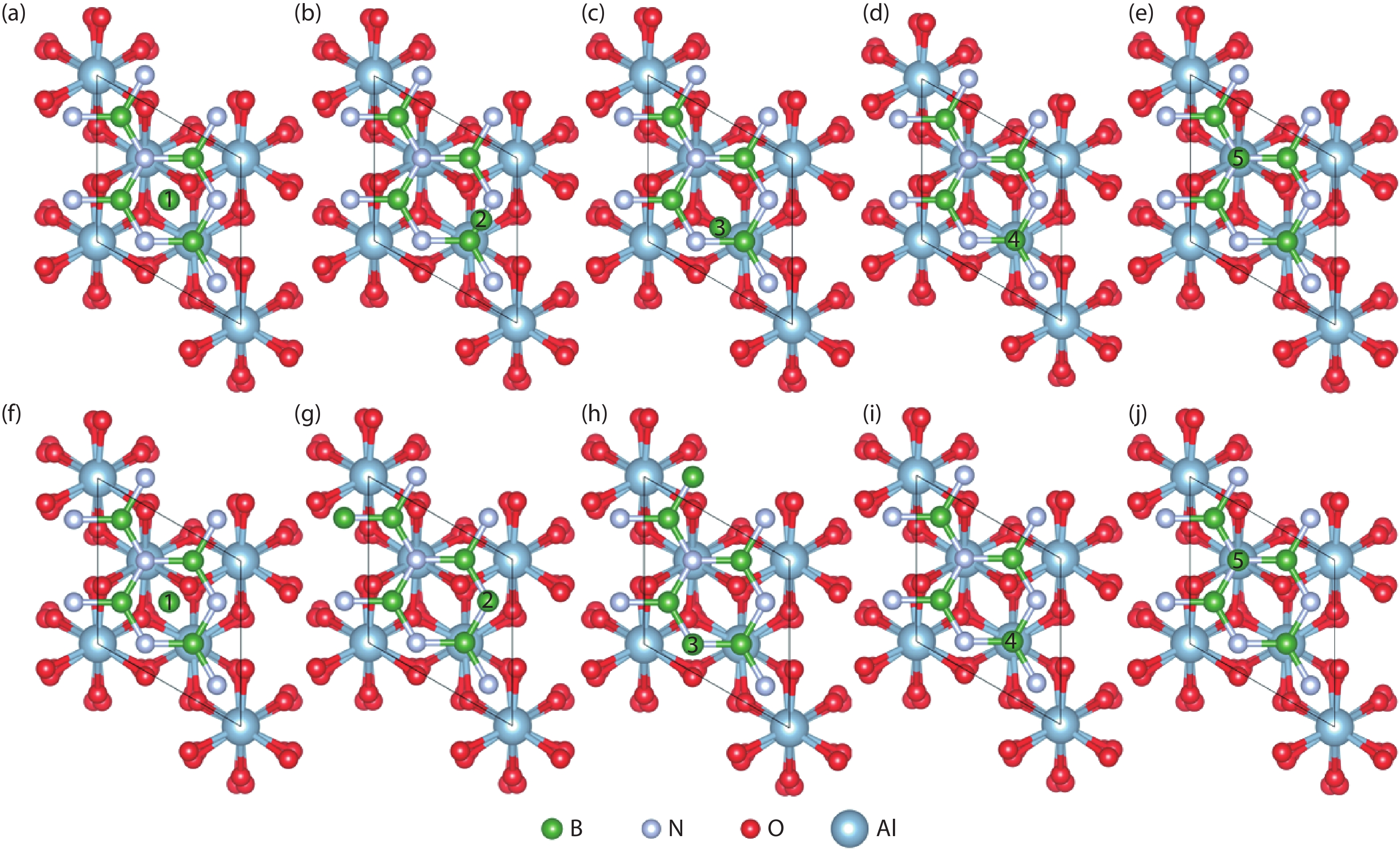
The initial absorption models of the free state B and N atoms at different absorption sites and the structures after the relaxation optimization of the surface atomic positions are shown in Fig. 1 and Fig. 2, respectively, where the five potential adsorption sites, i.e., S1–S5, are marked with numbers. All models adopt the heterojunction composed of Al2O3 (0001) plane with the same thickness and the single layer h-BN along the normal direction. After optimizing the positions of the free B and N atoms on the surface, three final adsorption sites were obtained for both cases. As shown in Table 1, for the free B atoms, the top site of N (SN-top) with the adsorption energy of –1.11 eV is the most stable adsorption site, which is the ideal growth site for the close packed structure of h-BN. The central site of the h-BN six-membered ring (SC) and the top site of B (SB-top) are two meta-stable sites with the adsorption energies of –0.87 and –0.76 eV, respectively. We note that the SC corresponds to the growth site of rhombohedral structure boron nitride (r-BN)[
![]()
Figure 1.(Color online) The top view of free B atoms at different adsorption sites with one h-BN buffer layer. (a–e) show the initial adsorption sites and (f–j) show the final configurations after optimization.
![]()
Figure 2.(Color online) The top view of free N atoms at different adsorption sites with one h-BN buffer layer. (a–e) show the initial adsorption sites and (f–j) show the final configurations after optimization.
Table Infomation Is Not EnableAfter calculating the relationship between the adsorption sites and the formation energy, we investigated the influence of the number of h-BN buffer layer on the formation energy. The Al2O3/h-BN-buffer-layer models with different numbers of buffer layer are shown in Fig. 3 for B and Fig. 4 for N atoms respectively. The SC site is chosen as the initial absorption site for the free B and N atoms. By structural relaxation, the adsorption energies with different buffer layers were gathered in Table 2, and the final adsorption positions of B and N atoms on the surface were shown in Fig. 3 and Fig. 4, respectively. In general, the formation energy increases as the number of buffer layer increases. For B atom, the adsorption site after relaxation is not changed as the number of buffer layer increases from 1 to 3. But for the N atom, the final adsorption site for the N atom is changed to the SN-top’ site only with 1 buffer layer. As the buffer layer increases to 2 or 3, the initial SC site for N atom is not changed. Both for the B and N atoms, the adsorption energy increases gradually as the number of buffer layer increases. When the number of h-BN buffer layer increases to 3, the adsorption process changes from an exothermic reaction to an endothermic reaction. As is known, during the growth process of h-BN, adjacent B and N atoms in the same atomic layer are combined to form a B–N bond by sp2 hybridization, and the inter layers are combined by van der Waals forces[
![]()
Figure 3.(Color online) (a–c) The top view and (d–f) front view of the optimized adsorption positions for B atom on the surface with different buffer layers. The SC site is chosen as the initial absorption site for the B atom.
![]()
Figure 4.(Color online) (a–c) The top view and (d–f) front view of the optimized adsorption positions for the N atom on the surface with different buffer layers. The SC site is chosen as the initial absorption site for the B atom.
Table Infomation Is Not EnableIn addition to calculating the formation energy of one isolate B or N atom on the surface, we also set up a pair of free B and N atoms on the surface with one h-BN buffer layer. The calculated formation energy is –3.11 eV. Compared to the formation energies of isolate B and N atoms at their adsorption site, the formation energy of the coexisting B and N atoms are much lower, indicating that B and N atoms can interact with each other on the surface to form B–N bond. Namely, the free B and N atoms firstly bond with each other and then combine with the adsorption sites of the h-BN buffer layer.
The diffusion of free B and N atoms on the buffer layer surface was simulated by the first-principles molecular dynamics. The probability distribution functions of atomic displacements projected onto the xy plane is shown in Fig. 5 to trace the diffusion of B and N atoms in the surface. At room temperature, the B and N atoms both show a relative localization distribution. In general, the B and N atoms tend to diffuse around the SN-top site and SB-top site respectively by overcoming the energy barrier between the adjacent adsorption sites. As shown in Figs. 5(a) and 5(b), the trajectory of the N atom is more localized than that of B atom, which is more likely to jump between two adjacent adsorption sites. This can be compared quantitatively by calculating the MSD and diffusion coefficient of B and N atoms according to Eqs. (2) and (3). According to Fig. 6 and Table 3, the B atom has a larger MSD with respect to the N atom. As a result, the diffusion coefficient of B atom is 1.07 × 10⁻⁹ m2/s at 300 K, much higher than 0.35 × 10⁻⁹ m2/s of N atom. As temperature increases to 1573 K, the activity of B and N atom are both increased and the distribution range is obviously expanded, as shown in Figs. 5(c) and 5(d). The diffusion of B atom is delocalized, which can diffuse freely on the surface by overcoming the energy barrier between the most stable and meta-stable sites. Although the distribution of N atom also shows delocalization characteristics, the trajectory is limited between specific adsorption sites. The N atom tends to diffuse across the sites around the B–N bond, increasing the probability of N bonding with N and B atoms in the buffer layer. The MSD of B atom is still larger than that of the N atom. The diffusion coefficients of B and N atoms at 1573 K increase to 17.04 × 10⁻⁹ and 7.18 × 10⁻⁹ m2/s, respectively. The diffusion rate of B atom is much higher than that of the N atom. It can thus be concluded that B atoms play a leading role in the growth process of h-BN. At high temperature, B atoms distribute uniformly at the growth sites by diffusion, then promoting N atoms to the break away from the localization to form B–N bonds.
![]()
Figure 5.(Color online) The probability distribution functions of atomic displacements projected onto the
![]()
Figure 6.The MSD curves of (a) B atoms and (b) N atoms on the buffer layer surface at different temperatures.
Table Infomation Is Not Enable4. Conclusion
In summary, we studied the growth and diffusion of B and N atoms on the surface of the Al2O3/h-BN-buffer-layer through first-principles calculations based on the density functional theory. The results show that the surface of single-buffer-layer h-BN provides several metastable adsorption sites for free B and N atoms due to the exothermic reaction. The free B atoms have the lowest adsorption energy at the adsorption site of the ideal growth point for h-BN, but the free N atoms are most easily to be trapped by the N atoms on the h-BN buffer layer to form the N–N bonds. As the number of buffer layer increases, the binding capacity of the surface of the buffer layer with free B and N atoms decreases. When the number of the h-BN buffer layer increases to three, the adsorption of the free B and N atoms on the surface changes from an exothermic reaction to an endothermic reaction. The influence of the Al2O3 substrate on the surface atoms is largely weakened. As temperature increases from 300 to 1573 K, the activity and diffusion range of B and N atoms increase significantly. The B atoms can diffuse freely on the buffer layer surface by overcoming the energy barrier between the adsorption sites. But the diffusion trajectory of N atoms is restricted in the specific adsorption sites around the B–N bonds of buffer layer. The B atoms play a major role in the formation of B–N bonds on the surface, the diffusion rate of which is much higher than that of the N atom. The introduction of buffer layers make the crystal growth have the characteristics of two-dimensional growth, which can effectively shield the negative effect of the substrate on the formation of B–N bonds. Also, they are conducive to the uniform diffusion surface B and N atoms, which can thus reduce the generation of the amorphous to improve the growth quality of h-BN.
Acknowledgements
This work was partly supported by the National Natural Science Foundation of China (61874007, 12074028), the Beijing Municipal Natural Science Foundation (4182046), Shandong Provincial Major Scientific and Technological Innovation Project (2019JZZY010209), Key-area research and the development program of Guangdong Province (2020B010172001), and the Fundamental Research Funds for the Central Universities (buctrc201802, buctrc201830, buctrc202127).
References
[1] A K Geim, K S Novoselov. The rise of graphene. Nat Mater, 6, 183(2007).
[2] J G Wang, X J Mu, X X Wang et al. The thermal and thermoelectric properties of in-plane C-BN hybrid structures and graphene/h-BN van der Waals heterostructures. Mater Today Phys, 5, 29(2018).
[3] Q Tang, Z Zhou. Graphene-analogous low-dimensional materials. Prog Mater Sci, 58, 1244(2013).
[4] J G Wang, F C Ma, M T Sun. Graphene, hexagonal boron nitride, and their heterostructures: Properties and applications. RSC Adv, 7, 16801(2017).
[5] Y X Song, C R Zhang, B Li et al. Triggering the atomic layers control of hexagonal boron nitride films. Appl Surf Sci, 313, 647(2014).
[6] R Dahal, J Li, S Majety et al. Epitaxially grown semiconducting hexagonal boron nitride as a deep ultraviolet photonic material. Appl Phys Lett, 98, 211110(2011).
[7] T C Doan, S Majety, S Grenadier et al. Fabrication and characterization of solid-state thermal neutron detectors based on hexagonal boron nitride epilayers. Nucl Instrum Methods Phys Res Sect A, 748, 84(2014).
[8] H X Jiang, J Y Lin. Hexagonal boron nitride for deep ultraviolet photonic devices. Semicond Sci Technol, 29, 084003(2014).
[9] L C Cai, X H Fan, H T Su et al. First principles calculation of the lattice constants of hexagonal and cubic boron nitride to 3000 K and 30 GPa. Ferroelectrics, 566, 136(2020).
[10] J Hafner. Ab-initio simulations of materials using VASP: Density-functional theory and beyond. J Comput Chem, 29, 2044(2008).
[11] D J Chadi. Special points for Brillouin-zone integrations. Phys Rev B, 16, 1746(1977).
[12] X Yang, S Nitta, K Nagamatsu et al. Growth of hexagonal boron nitride on sapphire substrate by pulsed-mode metalorganic vapor phase epitaxy. J Cryst Growth, 482, 1(2018).
[13] H Chikh, F SI Ahmed, A Afir et al.
[14] J H Wu, F Hagelberg, K Sattler. First-principles calculations of small silicon clusters adsorbed on a graphite surface. Phys Rev B, 72, 085441(2005).
[15] A Govind Rajan, M S Strano, D Blankschtein. Ab initio molecular dynamics and lattice dynamics-based force field for modeling hexagonal boron nitride in mechanical and interfacial applications. J Phys Chem Lett, 9, 1584(2018).
[16] A Zoroddu, F Bernardini, P Ruggerone et al. First-principles prediction of structure, energetics, formation enthalpy, elastic constants, polarization, and piezoelectric constants of AlN, GaN, and InN: Comparison of local and gradient-corrected density-functional theory. Phys Rev B, 64, 045208(2001).
[17] A Shigemi, T Wada. Enthalpy of formation of various phases and formation energy of point defects in perovskite-type NaNbO3 by first-principles calculation. Jpn J Appl Phys, 43, 6793(2004).
[18] I K Petrushenko, K B Petrushenko. Stone-Wales defects in graphene-like boron nitride-carbon heterostructures: Formation energies, structural properties, and reactivity. Comput Mater Sci, 128, 243(2017).
[19] S Nosé. A unified formulation of the constant temperature molecular dynamics methods. J Chem Phys, 81, 511(1984).
[20]
[21] M H Kowsari, S Alavi, M Ashrafizaadeh et al. Molecular dynamics simulation of imidazolium-based ionic liquids. I. Dynamics and diffusion coefficient. J Chem Phys, 129, 224508(2008).
[22] K Sadki, F Z Zanane, M Ouahman et al. Molecular dynamics study of pristine and defective hexagonal BN, SiC and SiGe monolayers. Mater Chem Phys, 242, 122474(2020).
[23] T Nagai, S Tsurumaki, R Urano et al. Position-dependent diffusion constant of molecules in heterogeneous systems as evaluated by the local mean squared displacement. J Chem Theory Comput, 16, 7239(2020).
[24] V R Manga, D R Poirier. Ab initio molecular dynamics simulation of self-diffusion in Al–Si binary melts. Model Simul Mater Sci Eng, 26, 065006(2018).
[25] M Chubarov, H Högberg, A Henry et al. Challenge in determining the crystal structure of epitaxial 0001 oriented sp 2 -BN films. J Vac Sci Technol A, 36, 030801(2018).
[26] D Skuridina, D V Dinh, M Pristovsek et al. Surface and crystal structure of nitridated sapphire substrates and their effect on polar InN layers. Appl Surf Sci, 307, 461(2014).
[27] F Dwikusuma, T F Kuech. X-ray photoelectron spectroscopic study on sapphire nitridation for GaN growth by hydride vapor phase epitaxy: Nitridation mechanism. J Appl Phys, 94, 5656(2003).

Set citation alerts for the article
Please enter your email address
© Copyright 2018-2021 | Chinese Laser Press. All Rights Reserved 沪ICP备15018463号-20