
Kai-Qi XU, Huang XU, Jia-Zhen ZHANG, Xiang-Dong WU, Lu-Han YANG, Jie ZHOU, Fang-Ting LIN, Lin WANG, Gang CHEN. Graphene/GaAs heterostructure based Millimeter/Terahertz wave photodetector[J]. Journal of Infrared and Millimeter Waves, 2020, 39(5): 533
- Journal of Infrared and Millimeter Waves
- Vol. 39, Issue 5, 533 (2020)
Abstract
Introduction
Sub-millimeter/THz wave photodetectors, due to its wide application in meteorology, astronomy, medicine, communication and biology[
Sub-millimeter and THz field effect transistors usually have submicron-scaled channel[
Graphene and other two-dimensional materials have been proven competent to detect long-wavelength photons in recent years[
1 Experimental
The high mobility GaAs sample was prepared with molecular beam epitaxial (MBE) method. Semi-insulating n-type GaAs wafer is used as the substrate. The growth is performed with a Riber-21 MBE system. After a high temperature adsorption of the substrate, a 50 nm GaAs layer, with the Si doping concentration of 2×1017 cm-3, is deposited at 600℃ with growth rate of 0.21 nm/s. Then the sample is taken out of the MBE chamber, and is cleaned using an ultrasonic treatment with acetone solution, isopropanol solution and deionized water. After drying with nitrogen, the sample is placed in oven, and is baked at 120 °C for another 2 hours.
Before transferring the graphene layer, a 10-nm-thick GaAs layer is etched away from the sample with a standard GaAs etching solution (H3PO4: H2O2: H2O = 40: 20: 400 ml). After that, single-layer graphene is transferred upon the substrate with a well-developed method21. Then we transferred a monolayer graphene sheet onto this substrate, which initially is grown on copper foil. The specific transfer process of graphene is as follows: Firstly, a layer of PMMA is spin coated onto the graphene film. Then it is put into a solution of ferric chloride (FeCl3) to etch the copper foil. After the copper foil is etched completely, it will be taken out and put into a dilute hydrochloric acid solution. The PMMA covered graphene is subsequently fished out by GaAs substrate. Finally, dip the hybrid graphene/GaAs sample is dipped into acetone solution to remove PMMA, and then it is further rinsed with isopropyl alcohol, and dried in the air.
Then the electrode source and drain are deposited (Cr/Au 5/60 nm) with ultraviolet lithography and electron beam evaporation. Graphene is etched with O2 plasma treatment to obtain designed channel size. After that, a 30nm-thick gate dielectric Al2O3 layeris deposited in ALD process. At last, electrode gate is deposited with ultraviolet lithography and electron beam evaporation process.
The IV characteristics of the devices were measured by B2912A Semiconductor Analyzer using variable voltage mode. For photoresponse measurements, the sub-millimeter/THz waves at different frequencies were generated from multiplier of electronic source and the photovoltage data were collected by B2912A and magnified by a lock-in amplifier and preamplifier. The 0.12 THz source based on frequency multipliers was employed in the photoresponse experiments. And the power density of the millimeter wave is 2.5 mW·cm-2, the power density of the sub-millimeter/THz radiation was 1.05 mW·cm-2 calibrated by a Golay cell. The detailed measurement setup can found in our previous work[
2 Results and discussion
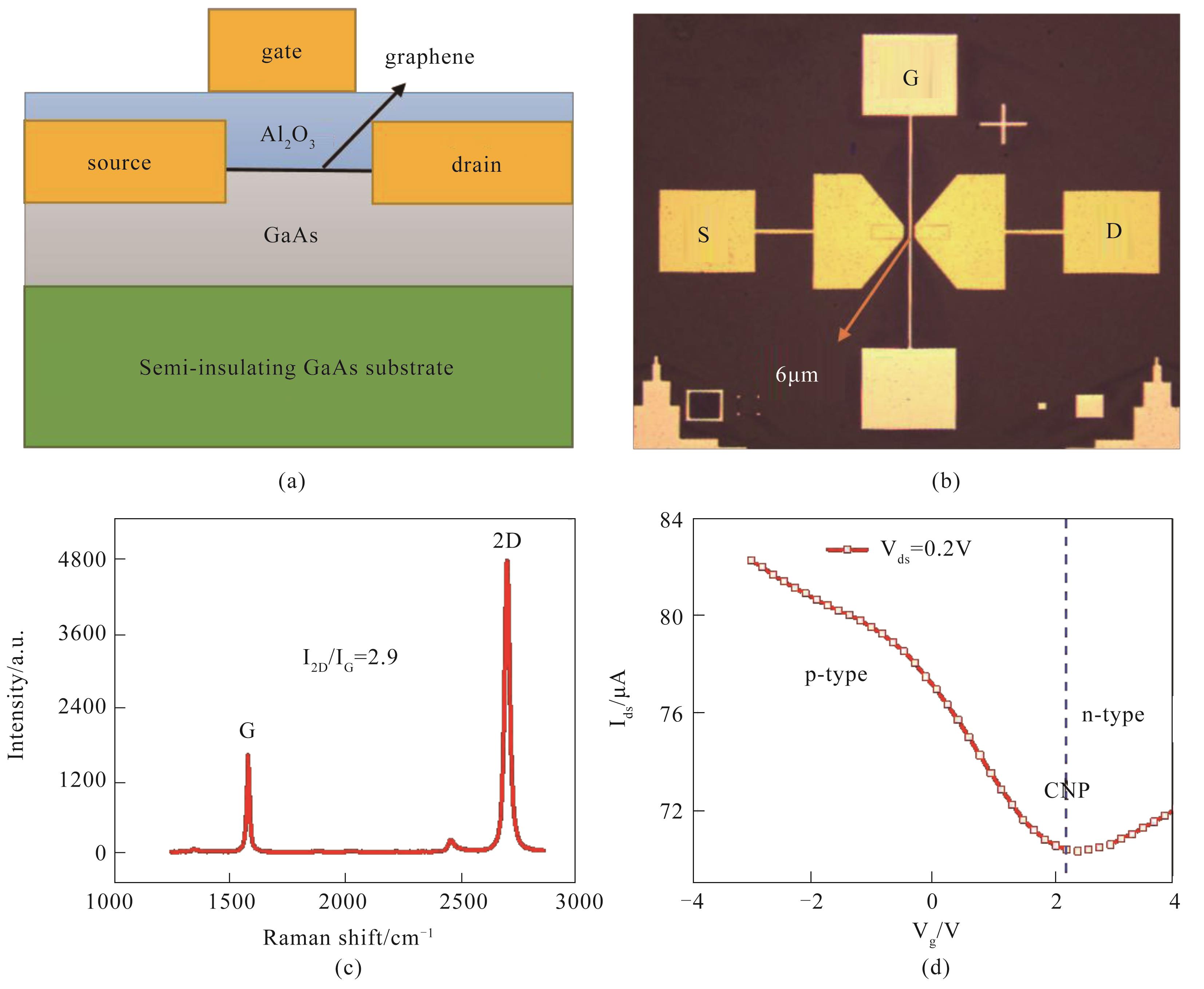
Fig.1(a), (b) are the cross-sectional structural schematic and the corresponding optical top view of the fabricated device, respectively. Here, the graphene channel length is L = 6 μm. To enhance the absorption at wavelength of millimeter scale, a bow-tie antenna with subwavelength gap is contacted to the detecting material to form the channel. The length and the width of the bow-tie antenna defined region are 200 μm and 140 μm, respectively, as shown in Fig. 1(b). In Fig.1(c) Raman spectrum of the monolayer graphene shows two strong peaks: 2D peak (2680 cm-1) and G peak (1580 cm-1), which indicates the high quality of the monolayer graphene, since 2D/G intensity ratio is about 2.9. The D peak at 1350 m-1) is caused by the disorder induction and defect of graphene. The peak value is small, indicating that the quality of transferred graphene is high24-26. As shown in Fig.1(d), the transfer characteristic curve of the detector shows a bipolar behavior27. The neutral charge point (CNP) is located at Vg (gate voltage) = 2.2 V, indicating that graphene is p-type.
![]()
Figure 1.(a) (b) the cross-sectional structural schematic and the corresponding optical top view of the fabricated device (c) Raman spectrum of the monolayer graphene (d) transfer characteristic curve measured with Vds = 0.2V
Fig.2(a) (b) are the time response of the photocurrent under radiation of 25 GHz at modulation frequencies of 1 kHz and 10 kHz with zero bias. Fig.2(c) is the photocurrent response as a function of incident power at different bias voltages. It can be seen that the photocurrent increases almost linearly with the incident light power, which is due to fact that the higher the incident light power, the more pairs of electron-hole and excitons are generated. Fig.2 (d) shows the time response of the photocurrent at different bias voltage. The time response is still smooth at the modulation frequency reached 1kHz and 10 kHz. It indicated that the response performance of the device is at μs level, which will be discussed later.
![]()
Figure 2.(a) (b) Time response of the photocurrent under radiation of 25 GHz at modulation frequencies of 1kHz and 10kHz with zero bias (c) Photocurrent response as a function of incident power at different bias voltages (d) Time response of the photocurrent at different bias voltage
Fig.3(a) is the extension of the rising edge and falling edge (inset) of the photocurrent in a single time-period. And the rising time and falling time are 9.8 µs and 2 µs, respectively, which is usually defined as the time measured from 10% up to 90% on rising edge of signal as well as the recovery time from 90% down to 10% of the falling edge. In the meantime, the response speed is also much faster than the typical RT thermal-based photodetectors such as the pyroelectric and bolometric ones, which response to the radiation on the order of ms. Fig.3(b) is the photocurrent as a function of the gate voltage with Vds of 0.2 V, which will be discussed with Fig.5(b) together later. It can be seen from Fig.3(c) that when the forward bias increases, the photocurrent increases almost linearly. And when reverse bias increases, the photo-current decreases linearly as well. Responsivity (Rv) and noise equivalent power (NEP) are two important parameters for photodetectors. Usually, a responsivity of Ri can be obtained from the equation Ri = (Sb·Iph) / (Pin·Sλ)at zero bias. Here Pin is the total power of the source, Sbis the radiation beam spot area, and is the active area. Nevertheless, given the fact that the wavelength λ corresponding to the 25 GHz is about 12 mm, which is much larger than the device itself. Thus an alternative method to calculate the responsivity has to be used for the sub-wavelength case4, in which, the responsivity can be expressed by Ri = (Sb·Iph) / (Pin·Sλ’), where the Sλ’= λ2/4. By this method, the Ri can be determined to be about 4.1 mA/W. Since the Rv = Ri∙R, R = 2.6 kΩ is the resistance of the device, the Rv = 10.7 V/W can be obtained. When the photocurrent reaches(Iph) 6.16 μA, the Rv of the device can be determined to be 20.6 V/W under Vds = 0.4 V. According to the noise equivalent power formula NEP = (4TRKB )1/2/ Rv, where KB is the Boltzmann constant, T is the temperature, R is the device resistance28-31, the noise equivalent power (NEP) of the device at RT can reach below 3.2×10⁻¹⁰ W/Hz1/2.
![]()
Figure 3.(a) The extension of the rising edge and falling edge (inset) of the photocurrent in a single time-period (b) Photocurrent as a function of the gate voltage with
Fig.4(a) (b) (c) show the time response of the device under radiation of 0.12 THz at different modulation frequencies of 1kHz, 5kHz and 10kHz under zero bias, respectively. Fig.4(d) is the time response of the photodetector at different bias voltage with different modulation frequencies of 1kHz. As can be seen from the Fig.4, the photodetector is extremely sensitive to terahertz radiation with fast response speed, and maintains a complete pulse shape at modulation frequency of 10 kHz, which indicates stable temporal response performance.
![]()
Figure 4.(a) (b) (c) The time response of the device under radiation of 0.12 THz at different modulation frequencies of 1kHz, 5kHz and 10kHz under zero bias (d) The time response of the photodetector at different bias voltage at different modulation frequencies of 1kHz
Fig.5(a) is the extension of the rising edge and falling edge (inset) of the photocurrent in a single time-period, in which the response time are 11 µs and 10 µs under radiation of 0.12THz. Fig. 5(b) shows photocurrent variation as a function of gate voltage with Vds of 0.4 V, in which the highest photocurrent reaches 113nA. Based on the obtained photocurrent, the photoresponsivity at different Vds can be determined as shown in Fig. 5(c). With 0.12 THz radiation, the λ is 2.5mm, and thus the responsivity at RT can reach 4.6V/W at Vds of 0.4 V. Similarly noise equivalent power can also be deduced and exhibited in Fig. 5(d) as a function of the gate voltage Vg, which shows the lowest NEP is less than 1.4×10⁻⁹ W Hz-1/2.
As shown in Fig. 3(b) and 5(b), the photocurrent of is mainly generated due to the intraband excitation of graphene. The contact potential does not contribute much to the photocurrent. It is necessary to consider the influence of high concentration carriers in GaAs on the photoresponse of graphene.
![]()
Figure 5.(a) The extension of the rising edge and falling edge (inset) of the photocurrent in a single time-period (b) Photocurrent variation as a function of gate voltage with Vds of 0.4 V (c) Photoresponsivity obtained at different bias voltage Vds (d) Noise equivalent power variation with the gate voltage Vg
To explore the mechanism behind the phenomena observed in the heterostructure-based photodetector, a schematic is proposed in Fig. 6, based on the measured responsivity as shown in Fig .1 and Fig. 3. Due to the nature of the hybrid channel of our device, the measured transfer characteristics is not only determined by the graphene[
![]()
Figure 6.Schematic energy band diagrams of graphene /GaAs hetero-structure (a) without millimeter/THz radiation; and (b) under millimeter/THz radiation
When the graphene is in contacting with GaAs, a contact potential well is formed, which leads to the accumulation of a number of carriers at the well. And the change in the size of the well will affect the carrier behavior between the source and the drain. Without millimeter/THz radiation, when Vds = 0.2 V, and Vg < 0, as shown in Fig. 1(c), the graphene Fermi level rises, leading to the rise of both of the barrier height between the graphene and the GaAs. Thus the carrier concentration at the potential well increases subsequently, resulting in the photocurrent Ids increases as well, as indicated in the Fig. 6(a). On the other hand, when 0 < Vg < 2.2 V, the graphene Fermi level decreases, which lowers the barrier as well as the carrier concentration, and the source and drain current decreases subsequently. Further increase the Vg above the neutral charge point of 2.2 eV, the inversion onsets, in which case, the graphene becomes n type, and the carrier concentration increases again.
On the other hand, under the radiation, the photocurrent of the photodetector is mainly generated by the in-band excitation of graphene, as indicated in Fig. 6(b). When Vg=0, the carriers accumulated in the contact well have a certain gain effect on the photocurrent due to the positive effect of the high concentration carriers in GaAs. When Vg<0, the potential well increases, and carriers at the potential well are difficult to migrate, which reduces the potentiation on the graphene photocurrent, and the photocurrent decreases. On the contrary, when Vg>0, the potential well is reduced, and the photocurrent potentiation on graphene is remarkable. When Vg>V(CNP), the photocurrent decreases, and changes to the contrary. Thus the results exhibited in Fig. 3 can be well understood.
3 Conclusion
In this work, a graphene/GaAs heterostructure based photodetector has been designed and fabricated, in which the two-dimensional electron gas characteristics are enhanced to improve the photoresponsivity at the band of millimeter and THz wave ranging from 20 GHz to 0.12 THz. Under 25 GHz radiation, the responsivity of photodetector at room temperature (RT) reaches 20.6V·W-1, with the response time of 9.8 μs and the noise equivalent power (NEP) of 3.2×10¹⁰ W·Hz-1/2 under a bias of 400 mV. At 0.12 THz, the responsivity is determined to be 4.6 V·W-1, with the response time of 10 μs. And a NEP of 1.4×10⁻⁹ W·Hz-1/2 can be achieved under the bias of 400 mV. To further improve the performance the GaAs/Graphene hetero-structured photodetector, various approaches will be adopted, such like optimization of the antenna, and the reducing the length of the channel, both to enhance the coupling of the electromagnetic field in the channel. These results exhibit great application potential for the graphene/GaAs heterostructure based Terahertz photodetectors.
References
[1] W. Monch. On the physics of metal-semiconductor interfaces. Reports on Progress in Physics, 53, 221-278(1990).
[2] H Liu, C Song, A Springthorpe et al. Terahertz quantum-well photodetector. Applied Physics Letters, 84, 4068-4070(2004).
[3] S Kopylov, A Tzalenchuk, S Kubatkin et al. Charge transfer between epitaxial graphene and silicon carbide. Applied Physics Letters, 97(2010).
[4] L Vicarelli, M S Vitiello, D Coquillat et al. Graphene field-effect transistors as room-temperature terahertz detectors. Nature Materials, 11, 865-871(2012).
[5] W Knap, F Teppe, Y Meziani et al. Plasma wave detection of sub-terahertz and terahertz radiation by silicon field-effect transistors. Applied Physics Letters, 85, 675-677(2004).
[6] K Peng, P Parkinson, L Fu et al. Single Nanowire Photoconductive Terahertz Detectors. Nano Letters, 15, 206-210(2015).
[7] Dyakonov, Michael, M. Shur. Shallow water analogy for a ballistic field effect transistor: New mechanism of plasma wave generation by dc current. Physical Review Letters, 71, 2465-2468(1993).
[8] C W Berry, N Wang, M R Hashemi et al. Significant performance enhancement in photoconductive terahertz optoelectronics by incorporating plasmonic contact electrodes. Nature Communications(4).
[9] E Castro-Camus, J Lloyd-Hughes, M B Johnston et al. Polarization-sensitive terahertz detection by multicontact photoconductive receivers. Applied Physics Letters, 86(2005).
[10] F H L Koppens, T Mueller, P Avouris et al. Photodetectors based on graphene, other two-dimensional materials and hybrid systems. Nature Nanotechnology, 9, 780-793(2014).
[11] X Cai, A B Sushkov, R J Suess et al. Sensitive room-temperature terahertz detection via the photothermoelectric effect in graphene. Nature Nanotechnology, 9, 814-819(2014).
[12] L Viti, J Hu, Coquillat, Dominique.. Black Phosphorus Terahertz Photodetectors. Advanced Materials, 27, 5567-5572(2015).
[13] J Yan, M H Kim, J A Elle et al. Dual-gated bilayer graphene hot-electron bolometer. Nature Nanotechnology, 7, 472-478(2012).
[14] Y F Lao, A G U Perera, L H Li et al. Tunable hot-carrier photodetection beyond the bandgap spectral limit. Nature Photonics, 8, 412-418(2014).
[15] Y J Hong, J W Yang, W H Lee et al. Van der Waals epitaxial double heterostructure: InAs/single-layer graphene/InAs. Advanced Materials, 25, 6914-6914(2013).
[16] S Chen, Z Han, M M Elahi et al. Electron optics with p-n junctions in ballistic graphene. Science Letter, 353, 1522-1525(2016).
[17] A K J S Geim. Graphene: status and prospects. science, 324, 1530-1534(2009).
[18] X Li, W Chen, P Wang et al. 18.5% Efficient graphene/GaAs van der Waals heterostructure solar cell. Nano Energy, 16, 310-319(2015).
[19] R R Nair, P Blake, Grigorenko et al. Fine structure constant defines visual transparency of graphene. Science, 320, 1308-1308(2008).
[20] K Rezgui, R Othmen, A Cavanna et al. The improvement of InAs/GaAs quantum dot properties capped by Graphene. Journal of Raman Spectroscopy, 44, 1529-1533(2013).
[21] J Wu, Z Yang, C Qiu et al. Enhanced performance of a graphene/GaAs self-driven near-infrared photodetector with upconversion nanoparticles. Nanoscale, 10, 8023-8030(2018).
[22] M Jiang, H Y Xiao, S M Peng et al. A comparative study of low energy radiation response of AlAs, GaAs and GaAs/AlAs superlattice and the damage effects on their electronic structures. Scientific reports, 8, 2012(2018).
[23] Q L Liu, Z Y Zhao, J H Yi. Interfacial interaction and effects of GaAs/Graphene hetero-structures studied by First-principle calculations. Journal of Alloys and Compounds, 795, 351-360(2019).
[24] Zhi Ting Hu, Tao Gan, Lei Du et al. A novel photodetector based on Graphene/InAs quantum dots/GaAs hetero-junction. Journal of Infrared and Millimeter Waves, 38(2019).
[25] A C Ferrari, J C Meyer, V. Scardaci et al. Raman spectrum of graphene and graphene layers. Phys Rev Lett, 97, 187401(2006).
[26] L M Malard, M A Pimenta, G Dresselhaus et al. Raman spectroscopy in graphene. Physics Reports, 473, 51-87(2009).
[27] F Tuinstra, J L Koenig. Raman Spectrum of Graphite. The Journal of Chemical Physics, 53, 1126-1130(1970).
[28] X Yang, J Sun, Qin et al. Room-temperature terahertz detection based on CVD graphene transistor. Chinese Physics B, 24, 47206-047206(2015).
[29] P L Richards. Bolometers for infrared and millimeter waves. J. Appl. Phys, 76, 1-24(1994).
[30] R Tauk, F Teppe, S Boubanga et al. Plasma wave detection of terahertz radiation by silicon field effects transistors: Responsivity and noise equivalent power. Applied Physics Letters, 89(2006).
[31] W Tang, A Politano, C Guo et al. Ultrasensitive Room-Temperature Terahertz Direct Detection Based on a Bismuth Selenide Topological Insulator. Advanced Functional Materials, 28, 1801786(2018).
[32] C Liu, L Du, W Tang et al. Towards sensitive terahertz detection via thermoelectric manipulation using graphene transistors. Npg Asia Materials, 318-327(2018).
[33] J Wu, Z Yang, C Qiu et al. Junction investigation of graphene/silicon Schottky diodes. Nanoscale research letters, 7, 302-302(2012).
[34] H Mark et al.

Set citation alerts for the article
Please enter your email address
© Copyright 2018-2021 | Chinese Laser Press. All Rights Reserved 沪ICP备15018463号-20