• Journal of Semiconductors
  • Vol. 42, Issue 9, 092001 (2021)
Di Wang, Zucheng Zhang, Bo Li, and Xidong Duan
Author Affiliations
  • Hunan Key Laboratory of Two-Dimensional Materials, State Key Laboratory for Chemo/Biosensing and Chemometrics, College of Chemistry and Chemical Engineering, Hunan University, Changsha 410082, China
  • show less
    DOI: 10.1088/1674-4926/42/9/092001 Cite this Article
    Di Wang, Zucheng Zhang, Bo Li, Xidong Duan. Synthesis of two-dimensional/one-dimensional heterostructures with tunable width[J]. Journal of Semiconductors, 2021, 42(9): 092001 Copy Citation Text show less
    (Color online) Schematic of a modified bidirectional flow CVD system.
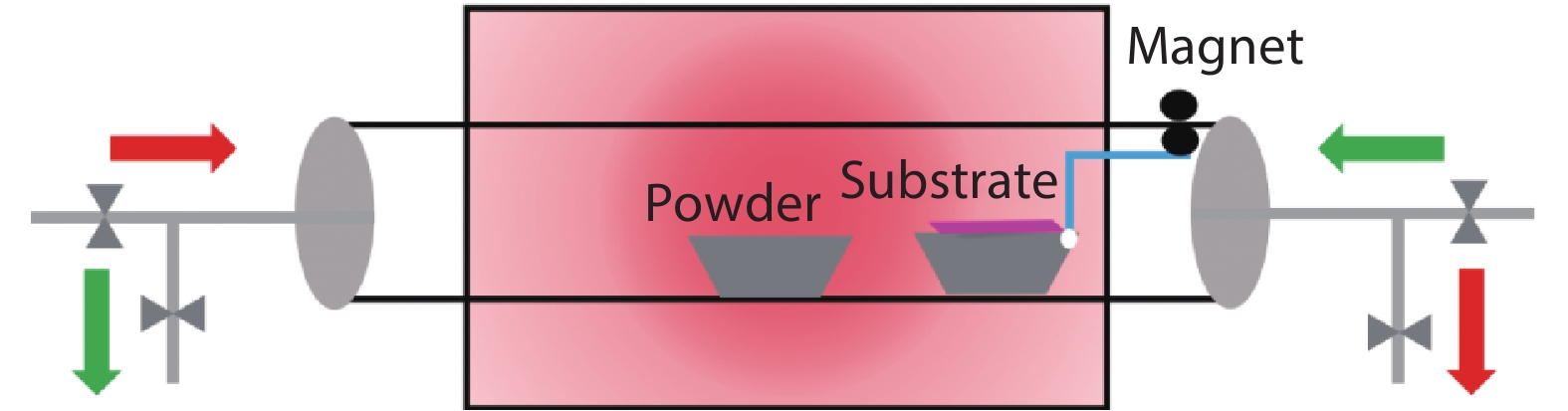
    Fig. 1. (Color online) Schematic of a modified bidirectional flow CVD system.
    (Color online) (a) Optical image of monolayer WS2. (b) PL spectrum of WS2. (c) Raman spectrum of WS2. (d) Optical image of WS2 in the yellow rectangle of (a). (e) PL mapping image of monolayer WS2. (f) Raman mapping image of monolayer WS2.
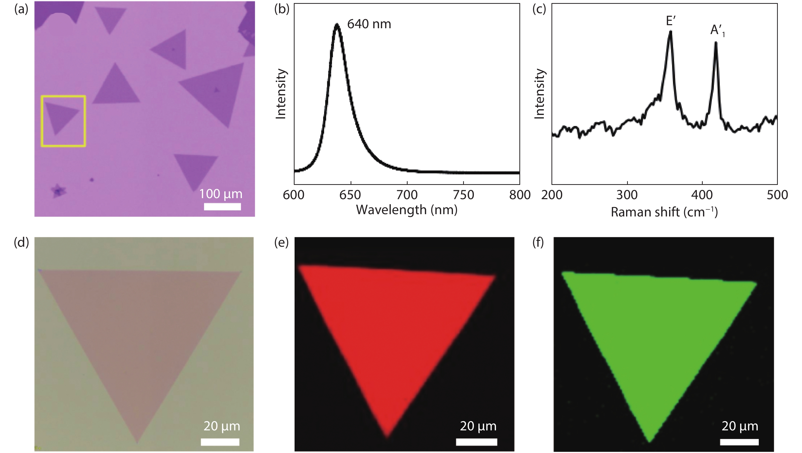
    Fig. 2. (Color online) (a) Optical image of monolayer WS2. (b) PL spectrum of WS2. (c) Raman spectrum of WS2. (d) Optical image of WS2 in the yellow rectangle of (a). (e) PL mapping image of monolayer WS2. (f) Raman mapping image of monolayer WS2.
    (Color online) AFM images of WS2/WSe2 lateral heterostructure when the growth time are (a) 5 s, (b) 7 s, (c) 9 s, (d) 11 s, (e) 30 s and (f) 40 s.
    Fig. 3. (Color online) AFM images of WS2/WSe2 lateral heterostructure when the growth time are (a) 5 s, (b) 7 s, (c) 9 s, (d) 11 s, (e) 30 s and (f) 40 s.
    SEM image of the 2D/1D WS2/WSe2 lateral heterostructure.
    Fig. 4. SEM image of the 2D/1D WS2/WSe2 lateral heterostructure.
    (Color online) AFM phase image of WS2/MoS2 lateral heterostructure when the growth time are (a) 3 min, (b) 1 min, and (c) 30 s.
    Fig. 5. (Color online) AFM phase image of WS2/MoS2 lateral heterostructure when the growth time are (a) 3 min, (b) 1 min, and (c) 30 s.
    (Color online) Raman and PL spectrum of WS2/MoS2 and WS2/WSe2 heterostructures. (a) Raman spectrum of the WS2/MoS2 heterostructure. (b) PL spectrum of the WS2/MoS2 heterostructure. (c) Raman spectrum of the WS2/WSe2 heterostructure. (d) PL spectrum of the WS2/WSe2 heterostructure.
    Fig. 6. (Color online) Raman and PL spectrum of WS2/MoS2 and WS2/WSe2 heterostructures. (a) Raman spectrum of the WS2/MoS2 heterostructure. (b) PL spectrum of the WS2/MoS2 heterostructure. (c) Raman spectrum of the WS2/WSe2 heterostructure. (d) PL spectrum of the WS2/WSe2 heterostructure.
    Di Wang, Zucheng Zhang, Bo Li, Xidong Duan. Synthesis of two-dimensional/one-dimensional heterostructures with tunable width[J]. Journal of Semiconductors, 2021, 42(9): 092001
    Download Citation