
Di Wang, Zucheng Zhang, Bo Li, Xidong Duan. Synthesis of two-dimensional/one-dimensional heterostructures with tunable width[J]. Journal of Semiconductors, 2021, 42(9): 092001
- Journal of Semiconductors
- Vol. 42, Issue 9, 092001 (2021)
Abstract
1. Introduction
Nanowires, as a kind of one-dimensional (1D) nanostructure, have been studied for many years. As early as 1995, William et al. has synthesized InP, InAs, and GaAs nanowhiskers by a solution–liquid–solid method[
The problem of lattice mismatch is often faced when 2D materials are combined into a heterostructure, but the appearance of 1D nanowires solves this problem. Recently, heterostructures composed of 1D materials and 2D materials have attracted much attention due to their promising application in electronic and optoelectronic devices. For instance, Qin et al. reported the synthesis of 1D Mo6Te6−2D MoTe2 heterostructures via the molecular beam epitaxy (MBE) method, which provides a new approach to synthesize 1D semimetallic nanowires[
Herein, we successfully synthesize 2D/1D WS2/WSe2 (WS2/MoS2) lateral heterostructures via a home-built bidirectional airflow CVD reactor in which the width of the WSe2 (MoS2) can be controlled by controlling air flow direction and growth time. Scanning electron microscope (SEM) and atomic force microscopy (AFM) images show that the width of the WSe2 can be tuned from 11 nm to 4 µm by precisely controlling the growth time. The interface of the 2D/1D heterostructures is clear and sharp. We also control the width of MoS2 in the same way. Our research provides a new method for the synthesis of 1D nanowires and lays the foundation for the future study of 2D/1D lateral heterostructures.
2. Methods
2.1. Synthesis of 2D WS2
WS2 nanosheets were first synthesized as substrates in our experiment. Different from the traditional CVD system, our reactor is equipped with four switches, which can pass two directions of air flow. At first, the WS2 powders were used as precursor and placed in the center of the heat zone. Meanwhile, the SiO2 (285 nm)/Si was placed at the low temperature zone. Next, 600 sccm Ar gas was introduced from the substrate to the precursor (green arrow, reverse flow) for about 20 min to clean the air in the quartz tube. Then, the flow rate was reduced to 75 sccm and the furnace was heated to 1200 °C in 40 min. When the temperature reached 1200 °C, we changed the direction of Ar gas to forward (red arrow) and kept it for 4 min. At last, the reactor was cooled to room temperature.
2.2. Synthesis of 2D/1D WS2/WSe2 heterostructures
At first, the WSe2 powders, as the precursor, were placed in the center of the heat zone. The SiO2/Si substrate with WS2 nanosheets was placed in the low temperature zone to grow heterostructures. Next, 600 sccm Ar was introduced at about 20 min. Then, the flow rate was reduced to 120 sccm and the furnace was heated to 1150 °C in 35 min. When the temperature reached to 1150 °C, the direction of Ar gas was changed and kept for 0–40 s. Then we used magnets and quartz hooks to pull the boat out quickly and turned the air flow back into the reverse direction. At last, the reactor was cooled to room temperature.
2.3. Synthesis of 2D/1D WS2/MoS2 heterostructures
Similarly, MoS2 powders were placed in the center of the heat zone and the SiO2/Si substrate with WS2 nanosheets was placed at the downstream. Next, 600 sccm Ar was introduced. Then, the flow rate was reduced to 120 sccm and the furnace was heated to 1190 °C in 40 min. When the temperature reached to 1190 °C, the direction of Ar gas was changed and kept for 0.5–3 min. Then we used magnets and quartz hooks to pull the boat out quickly and turned the air flow back into the reverse direction. At last, the reactor was cooled to room temperature.
2.4. Material characterization
The Raman and PL spectra images were conducted via a laser micro-Raman spectrometer (Renishaw Invia). The width of the heterostructure was measured by AFM (Bruker model: Dimension ICON) and SEM (TESCAN MIRA3).
3. Result and discussion
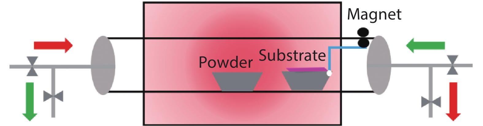
As shown in Fig. 1, we modified a bidirectional flow CVD process to precisely control the growth process that has been reported[
![]()
Figure 1.(Color online) Schematic of a modified bidirectional flow CVD system.
Because the heat resistance of WS2 is better than that of WSe2, we choose WS2 as the growth substrate. As shown in Fig. 2(a), monolayer WS2 that we synthesized in the first step is about 100 µm. The uniform surface and sharp edge are suitable for the epitaxy of the second step. Fig. 2(b) shows that PL peak of monolayer WS2 locates at 640 nm, which is consistent with previous study[
![]()
Figure 2.(Color online) (a) Optical image of monolayer WS2. (b) PL spectrum of WS2. (c) Raman spectrum of WS2. (d) Optical image of WS2 in the yellow rectangle of (a). (e) PL mapping image of monolayer WS2. (f) Raman mapping image of monolayer WS2.
As shown in Fig. 3, the width of WSe2 of the WS2/WSe2 heterostructures can be sequentially tuned by controlling the air direction and growth time. When the growth time is controlled at 5 s, the WSe2 nanoribbons can be grown at the edge of WS2 with a width of 90 nm (Fig. 3(a)), which means that the 2D/1D WS2/WSe2 heterostructure is synthesized. With the prolongation of growth time, the width of WSe2 is increased to a few hundred nanometers (Figs. 3(b)–3(d)). As shown in Figs. 3(e) and 3(f), the width of WSe2 can be tuned larger than 1 µm when the growth time is 30 s. Moreover, it can be observed that the WS2/WSe2 heterostructures are clean and uniform, which are good for application.
![]()
Figure 3.(Color online) AFM images of WS2/WSe2 lateral heterostructure when the growth time are (a) 5 s, (b) 7 s, (c) 9 s, (d) 11 s, (e) 30 s and (f) 40 s.
In fact, there are some narrower nanoribbons at 0–3 s that are difficult to be characterized by AFM, so we conducted scanning electron microscopy (SEM) to characterize their widths. As shown in Fig. 4, the 11 nm wide WSe2 can be grown at the edge of WS2, which represents that an ultra-narrow nanowire was synthesized.
![]()
Figure 4.SEM image of the 2D/1D WS2/WSe2 lateral heterostructure.
To prove the universality of this approach, 2D/1D WS2/MoS2 lateral heterostructures were also synthesized by using the same method. Fig. 5(a) shows that the width of MoS2 is about 4 µm when the growth time is 3 min. When the growth time is reduced to 1 min, the width of MoS2 is reduced to 300 nm (Fig. 5(b)). As shown in Fig. 5(c), the width of MoS2 is reduced to 200 nm with the growth time reduced to 30 s. These results show that our method can control the width of a 2D/1D heterostructure simply and effectively.
![]()
Figure 5.(Color online) AFM phase image of WS2/MoS2 lateral heterostructure when the growth time are (a) 3 min, (b) 1 min, and (c) 30 s.
The Raman and PL analyses were conducted to further study the spectroscopy and photoluminescence performance of the as-grown lateral heterostructure. Fig. 6(a) shows the Raman spectra at three different locations of the WS2, WS2/MoS2 interface and MoS2. Two distinct peaks at 357 and 419 cm–1 in the Raman spectrum of WS2 (blue line) are consistent with those mentioned above. The Raman spectrum from the peripheral region display two peaks at 384 and 405 cm−1 (red line in Fig. 6(a)), in agreement with the E' and A1' resonance modes of MoS2[
![]()
Figure 6.(Color online) Raman and PL spectrum of WS2/MoS2 and WS2/WSe2 heterostructures. (a) Raman spectrum of the WS2/MoS2 heterostructure. (b) PL spectrum of the WS2/MoS2 heterostructure. (c) Raman spectrum of the WS2/WSe2 heterostructure. (d) PL spectrum of the WS2/WSe2 heterostructure.
4. Conclusion
In summary, we successfully synthesized 2D/1D WS2/WSe2 (WS2/MoS2) lateral heterostructures by a bidirectional flow CVD reactor. WSe2 and MoS2 with different widths can be epitaxially grown on the edge of WS2. The width of the WSe2 can be tuned from 11 nm to 4 µm by precisely controlling the growth time. AFM and SEM images show that the interface of the 2D/1D heterostructures is clear and smooth. Our investigation provides a new method for the preparation of ultranarrow 1D nanoribbons and breaks new ground in the future study of the 2D/1D lateral heterostructures.
Acknowledgements
The authors at Hunan University acknowledge the support from National Natural Science Foundation of China (No. 51872086), the Hunan Key Laboratory of Two-Dimensional Materials (Grant No. 2018TP1010) and the Innovative Research Groups of Hunan Province (Grant No. 2020JJ1001) for the work conducted at Hunan University.
References
[1] T J Trentler, K M Hickman, S C Goel et al. Solution-liquid-solid growth of crystalline III-V semiconductors: an analogy to vapor-liquid-solid growth. Science, 270, 1791(1995).
[2] R Yan, D Gargas, P Yang. Nanowire photonics. Nat Photon, 3, 569(2009).
[3] L X Zheng, M J O'Connell, S K Doorn et al. Ultralong single-wall carbon nanotubes. Nat Mater, 3, 673(2004).
[4] S Lei, L Ge, S Najmaei et al. Evolution of the electronic band structure and efficient photo-detection in atomic layers of InSe. Acs Nano, 8, 1263(2014).
[5] S M Poh, S J R Tan, X Zhao et al. Large area synthesis of 1D-MoSe2 using molecular beam epitaxy. Adv Mater, 29, 1605641(2017).
[6] R Qi, S Wang, M Wang et al. Towards well-defined MoS2 nanoribbons on a large scale. Chem Commun, 53, 9757(2017).
[7] S Li, Y C Lin, W Zhao et al. Vapour-liquid-solid growth of monolayer MoS2 nanoribbons. Nat Mater, 17, 535(2018).
[8] W Huang, X Wang, X Ji et al. In-situ fabrication of Mo6S6-nanowire-terminated edges in monolayer molybdenum disulfide. Nano Res, 11, 5849(2018).
[9] Y Zhou, J Dong, H Li et al. Electronic transport properties of in-plane heterostructures constructed by MoS2 and WS2 nanoribbons. RSC Adv, 5, 66852(2015).
[10] W Zhou, G Yu, A N Rudenko et al. Tunable half-metallicity and edge magnetism of H-saturated InSe nanoribbons. Phys Rev Mater, 2, 114001(2018).
[11] K X Chen, Z Y Luo, D C Mo et al. WSe2 nanoribbons: new high-performance thermoelectric materials. Phys Chem Chem Phys, 18, 16337(2016).
[12] M Wu, J J Shi, M Zhang et al. Modulation of electronic and magnetic properties in InSe nanoribbons: edge effect. Nanotechnology, 29, 205708(2018).
[13] G Z Magda, X Jin, I Hagymasi et al. Room-temperature magnetic order on zigzag edges of narrow graphene nanoribbons. Nature, 514, 608(2014).
[14] J J Wang, F F Cao, L Jiang et al. High performance photodetectors of individual InSe single crystalline nanowire. J Am Chem Soc, 131, 15602(2009).
[15] Y Yu, G Wang, Y Tan et al. Phase-controlled growth of one-dimensional Mo6Te6 nanowires and two-dimensional MoTe2 ultrathin films heterostructures. Nano Lett, 18, 675(2018).
[16] J Zhang, Y Wei, F Yao et al. SWCNT-MoS2-SWCNT vertical point heterostructures. Adv Mater, 29, 1604469(2017).
[17] D Jariwala, V K Sangwan, C C Wu et al. Gate-tunable carbon nanotube-MoS2 heterojunction p-n diode. Proc Natl Acad Sci USA, 110, 18076(2013).
[18] Y Liu, X He, D Hanlon et al. Liquid phase exfoliated MoS2 nanosheets percolated with carbon nanotubes for high volumetric/areal capacity sodium-ion batteries. Acs Nano, 10, 8821(2016).
[19] H Huang, W Huang, Z Yang et al. Strongly coupled MoS2 nanoflake-carbon nanotube nanocomposite as an excellent electrocatalyst for hydrogen evolution reaction. J Mater Chem A, 5, 1558(2017).
[20] Z Zhang, P Chen, X Duan et al. Robust epitaxial growth of two-dimensional heterostructures, multiheterostructures, and superlattices. Science, 357, 788(2017).
[21] X Duan, C Wang, J C Shaw et al. Lateral epitaxial growth of two-dimensional layered semiconductor heterojunctions. Nat Nanotechnol, 9, 1024(2014).
[22] A Berkdemir, H R Gutierrez, A R Botello-Mendez et al. Identification of individual and few layers of WS2 using Raman Spectroscopy. Sci Rep, 3, 1755(2013).
[23] A M van der Zande, P Y Huang, D A Chenet et al. Grains and grain boundaries in highly crystalline monolayer molybdenum disulphide. Nat Mater, 12, 554(2013).

Set citation alerts for the article
Please enter your email address
© Copyright 2018-2021 | Chinese Laser Press. All Rights Reserved 沪ICP备15018463号-20