
Yuxuan Ke, Yingqian Cen, Dianyu Qi, Wenjing Zhang, Qing Zhang. Two‑Dimensional Materials Photodetectors for Optical Communications[J]. Chinese Journal of Lasers, 2023, 50(1): 0113008
- Chinese Journal of Lasers
- Vol. 50, Issue 1, 0113008 (2023)
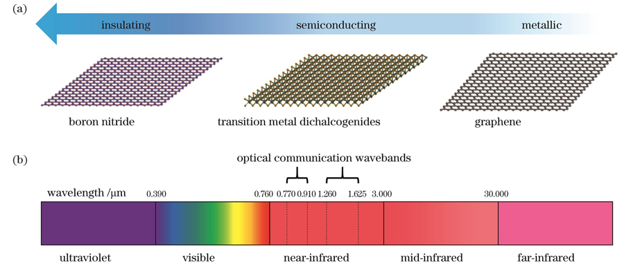
Fig. 1. Two-dimensional materials covering broad spectrum. (a) Schematics of structure and bandgap of boron nitride, transition metal dichalcogenides and graphene; (b) spectrum range from ultraviolet to far-infrared where optical communication waveband is in near-infrared range
![Graphene-based photodetectors for optical communications. (a) Schematic and scanning electron image (inset) of metal/graphene/metal (MGM) photodetectors with asymmetry metal contacts[53]; (b) schematic of graphene-based photodetector integrated on silicon optical waveguide with asymmetry contact[55]; (c) structural diagram of graphene-based photodetector on silicon substrate where silica between electrodes and substrate ensures collected carriers originating only from graphene[56]; (d) photocurrent and responsivity as functions of power under 1550 nm illumination[56]; (e) rising-edge photocurrent response as a function of time under 632 nm and 1550 nm illuminations, respectively[56]; (f) photocurrent as a function of time on graphene nanoribbon-based devices covered with and without hafnium oxide under 1470 nm illumination[57]](/richHtml/zgjg/2023/50/1/0113008/img_02.jpg)
Fig. 2. Graphene-based photodetectors for optical communications. (a) Schematic and scanning electron image (inset) of metal/graphene/metal (MGM) photodetectors with asymmetry metal contacts[53]; (b) schematic of graphene-based photodetector integrated on silicon optical waveguide with asymmetry contact[55]; (c) structural diagram of graphene-based photodetector on silicon substrate where silica between electrodes and substrate ensures collected carriers originating only from graphene[56]; (d) photocurrent and responsivity as functions of power under 1550 nm illumination[56]; (e) rising-edge photocurrent response as a function of time under 632 nm and 1550 nm illuminations, respectively[56]; (f) photocurrent as a function of time on graphene nanoribbon-based devices covered with and without hafnium oxide under 1470 nm illumination[57]
Fig. 3. BP-based photodetectors for optical communications. (a) Responsivity as a function of power density under 532 nm and 1550 nm illumination, respectively[41]; (b) BP photodetectors integrated on silicon optical waveguide where few-layer graphene is as top gate[40]
Fig. 4. Tellurium-based photodetectors for optical communications. (a) Structural diagram of tellurium photodetector based on optical cavity for short-wave infrared detection [59]; (b) responsivity as a function of wavelength under Al2O3 with different thicknesses[59]; (c) photocurrent as a function of power under 1550 nm illumination where fitting slope is 19.2 mA·W-1[60]; (d) structural diagram of photodetector based on tellurium[61]; (e) change rate of photoconductance as a function of time under 1550 nm illumination with power density of 150 mW·cm-2[61]; (f) rising-edge photoconductance response as a function of time under 1550 nm illumination with falling-edge photoconductance response as a function of time shown in inset[61]
Fig. 5. Germanium-, bismuth-, and arsenium-based photodetectors for optical communications. (a) Schematic of resonant-photonic crystal germanium photodetector[62]; (b) measured EQE as a function of wavelength for 30-μm-diameter patterned photodetectors with hole-array (hole diameter of 300 nm) period of 520-560 nm[62]; (c) 3D schematic of Bi photodetector[63]; (d) normalized responsivity for Bi photodetector as a function of wavelength[63]; (e) schematic of As-Si photodetector[64]; (f) EQE and responsivity for photodetector as functions of wavelength[64]
Fig. 6. MoS2- and MoTe2-based photodetectors for optical communications. (a) 3D schematic of triple-layer MoS2 photodetector[65]; (b) responsivity of MoS2 photodetector as a function of excitation wavelength[65]; (c) schematic of graphene/MoTe2/Au photodetector stacked onto silicon waveguide,which is encapsulated by large h-BN flake[66]; (d) wavelength dependence of responsivity for 19.5 nm thick and 50 nm thick photodetectors[66]; (e) frequency dependence of responsivity for MoTe2 photodetector with measurement setup shown in inset [66]; (f) schematic of silicon microring resonator-integrated MoTe2 photodetector (radius of 40 μm, height of 220 nm, width of 500 nm)[67]; (g) responsivity and EQE as functions of bias voltage for two devices (device 1 with thickness of 40 nm and coverage length of 15 μm and device 2 with thickness of 60 nm and coverage length of 30.7 μm) with magnified responsivity and EQE curves for device 1 shown in inset [67]; (h) photoresponse of type II Weyl semimetal MoTe2 photodetector under different excitation wavelengths[68]
Fig. 7. Noble metal dichalcogenides-based photodetectors for optical communications. (a) Schematic of palladium selenide-based photodetector integrated on silicon optical waveguide[69]; (b) responsivity as a function of bias voltage under 1550 nm illumination[69]; (c) photocurrent as a function of detecting wavelength under light power of 1 mW and bias voltage of 5 V[69]; (d) schematic of palladium selenide-based photodetector integrated with waveguide[70]; (e) frequency response curves of three palladium selenide photodetectors under bias of 3 V[70]; (f) responsivity and external quantum efficiency of three photodetectors as functions of bias voltage[70]; (g) schematic of palladium selenide photodetector on gold/titanium dioxide optical cavity substrate[11]; (h) photocurrent response as a function of time under 532 nm and 1550 nm illuminations, respectively[11]; (i) responsivity on platinum telluride photodetector as a function of wavelength[71]
Fig. 8. Bismuth selenide-based photodetectors for optical communications[27]. (a) Schematic of photodetector based on bismuth selenide; (b) photocurrent as a function of time under bias voltage of 1 V and light power of 142.93 mW/cm2 ; (c) responsivity and detectivity as functions of temperature; (d) rising time and decay time as functions of temperature
Fig. 9. Mo2C-based photodetectors for optical communications[73]. (a) Schematic of photodetectors based on MoS2/p-Mo2C hybrid structure under light illumination; (b) wavelength dependence of light-to-dark current ratio for MoS2 and MoS2/p-Mo2C (P=1000 nm) photodetectors; (c) wavelength dependences of responsivity and light-to-dark current ratio for MoS2 and MoS2/mp-Mo2C photodetectors
Fig. 10. Three types of energy band structures of heterojunctions
Fig. 11. vdWs heterojunction-based photodetectors for optical communications. (a) Schematic of device based on BP/MoS2 vdWs heterojunction[74]; (b) photocurrent response as a function of time at different bias voltages under incident light wavelength of 1550 nm and power of 96.2 μW[74]; (c) transfer curves under 1550 nm illumination with different powers[74]; (d) schematic of interlayer excitation process in MoTe2/MoS2 vdWs type II heterojunction[76]; (e) schematic of type II energy alignment and interlayer transition mechanism in GaTe/InSe vdWs heterojunction where Eg-p and Eg-n are bandgaps of p-GaTe and n-InSe, respectively[77]; (f) responsivity on GaTe, InSe and GaTe/InSe heterojunction devices as a function of detecting wavelength[77]; (g) responsivity and detectivity on WSe2/graphene/MoS2 heterojunction device as functions of detecting wavelength of 400-2400 nm[80]; schematics of optical absorption principle and band structure of heterojunction in (h) ultraviolet-visible and (i) infrared ranges[80]
|
Table 1. Summary of 2D materials photodetectors for optical communications

Set citation alerts for the article
Please enter your email address
© Copyright 2018-2021 | Chinese Laser Press. All Rights Reserved 沪ICP备15018463号-20