Emerging two-dimensional (2D) materials, including graphene, transition metal dichalcogenides, black phosphorus, and perovskites, have attracted considerable attention owing to their extraordinary physical and chemical properties. They are atomically thin, with no surface dangling bonds, good electrostatic tunability of carrier concentration, and strong light-matter interactions. These advantages make them promising materials for high-efficiency nanoscale photodetectors for optical chips. For instance, monolayer molybdenum disulfide (MoS2) can absorb 10% of light due to a large absorption coefficient of 107 m-1. Platinum diselenide (PtSe2) possesses high mobility of over 103 cm2·V-1·s-1 and a bandgap of 0.3-2.0 eV, which is promising for wide-band optical communication photodetectors. Meanwhile, the non-dangling surfaces of 2D materials enable van der Waals (vdWs) integration for various heterostructures without the constraint of crystal lattice mismatching.2D material photodetectors for optical communication, including single-element 2D materials, double-element 2D materials, and 2D heterostructures, have been extensively explored. They have demonstrated excellent performance, including high responsivity and detectivity, fast response time, and wide bandwidth. Despite the realization of these great successes, 2D photodetectors operating in optical communication bands still face many application challenges. Therefore, it is necessary to summarize the research progress and discuss the challenges of this important field.
For double-element 2D material photodetectors, higher responsivities were achieved than those of single-element photodetectors. For instance, Leuthold's group fabricated few-layer MoTe2 waveguide photodetectors with high responsivity (0.4 A/W), broad bandwidth (1 GHz), and fast data transmission rate (1 Gbit/s) using a graphene/MoTe2/Au structure. Zhai's group achieved Bi2Se3 photodetectors with high responsivity (2.7 A/W) and detectivity (3.3×1010 cm·Hz1/2·W-1) at the C-band. For 2D heterostructures, Park's group demonstrated ReS2/ReSe2 photodetectors with ultrahigh responsivity of 1.58×10⁵ A/W at the O-band. Zhang's group demonstrated GaTe/InSe photodetectors with a broad detection range (400-1600 nm) and high responsivity (2 A/W). Furthermore, Miao's group fabricated photodetectors with a broad detection range (400-1600 nm), high detectivity (11.7 A/W), and rapid response time (30.3 μs) using MoS2/graphene/WSe2 heterostructures. Finally, the challenges and ongoing research in this field are discussed, including scalable synthesis, low Schottky barriers for electrical contact, and high absorption.
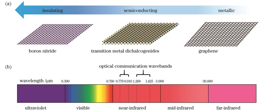
Photodetectors that convert a light signal into an electrical signal play an important role in optical communications, displays, and other such applications. Nanoscale photodetectors operating in the optical communication band are one of the most important research objects in optical chip technology. Optical communication bands contain two spectral ranges. One is called the 850 nm band from 770 nm to 910 nm; the photodetectors in this band mainly use technologically important Si semiconductors as photoactive materials. The other range includes the original (1260-1360 nm, O), extended-wavelength (1360-1460 nm, E), short-wavelength (1460-1530 nm, S), conventional (1530-1565 nm, C), long-wavelength (1565-1625 nm, L), and ultra-long-wavelength (1625-1675 nm, U) bands. The photodetectors in these bands use indium gallium arsenide (InGaAs) and mercury cadmium telluride (HgCdTe) as photoactive materials. However, they still suffer from complex and high-cost growth processes, low detection efficiency, and low operation temperature.
We first introduced the working principles and important characteristic parameters of photodetectors. The working principles include the effects of photoconductive, photovoltaic, photogating, and photo-thermoelectric properties. The characteristic parameters include the photocurrent, ON/OFF ratio, external quantum efficiency (EQE), and detectivity. Next, we discussed the research progress in photodetectors based on the 2D materials (single-element and double-element) and their heterostructures in optical communication bands (Table 1). For example, Avouris's group demonstrated a graphene photodetector with a 10 Gbit/s data transmission rate using the asymmetric metal contact technique. Xu's group demonstrated a graphene photodetector on silicon with high responsivity owing to the prolongation of the photon-generated carrier lifetime induced by the built-in field at the heterointerface between graphene and silicon. Mueller et al. demonstrated a graphene photodetector with ultrashort intrinsic response time of 2.1 ps using metal-graphene-metal structures. Javey's group designed optical cavity-enhanced tellurium photodetectors exhibiting a high responsivity (>2.5 A/W) within the entire optical communication bands (Fig. 4). Similarly, Song et al. fabricated bismuth-based photodetectors with high responsivity (0.62 A/W) and EQE (50%) at C band using photonic crystal-enhanced structures (Fig. 5).
2D material photodetectors have shown high responsivity and detectivity, fast response time, and wide bandwidth. This provides an effective strategy for the development of high-efficiency nanoscale photodetectors for next-generation optical chips and interconnections. We reviewed the recent progress made in 2D material photodetectors for optical communications. We focused on two types of material platforms: 1) 2D materials, including single- and double-element 2D materials, and 2) 2D heterostructures. Despite great progress, some challenges still exist for our ongoing exploration.