• Photonics Research
  • Vol. 10, Issue 12, 2768 (2022)
Wenkai Yang1、2、†, Lige Liu1、2、†, Dashan Dong1、2, Xin Zhang3, Han Lin4, Yunkun Wang1、2, Hong Yang1、2, Yunan Gao1、2, Haizheng Zhong3, Baohua Jia4, and Kebin Shi1、2、5、*
Author Affiliations
  • 1State Key Laboratory for Mesoscopic Physics and Frontiers Science Center for Nano-optoelectronics, School of Physics, Peking University, Beijing 100871, China
  • 2Collaborative Innovation Center of Extreme Optics, Shanxi University, Taiyuan 030006, China
  • 3MIIT Key Laboratory for Low-Dimensional Quantum Structure and Devices, School of Materials Sciences and Engineering, Beijing Institute of Technology, Beijing 100081, China
  • 4School of Science, RMIT University, Melbourne 3000, VIC, Australia
  • 5Peking University Yangtze Delta Institute of Optoelectronics, Nantong 226010, China
  • show less
    DOI: 10.1364/PRJ.472321 Cite this Article Set citation alerts
    Wenkai Yang, Lige Liu, Dashan Dong, Xin Zhang, Han Lin, Yunkun Wang, Hong Yang, Yunan Gao, Haizheng Zhong, Baohua Jia, Kebin Shi. Detour-phased perovskite ultrathin planar lens using direct femtosecond laser writing[J]. Photonics Research, 2022, 10(12): 2768 Copy Citation Text show less
    PUP lens design based on the detour phase method. (a) Schematic illustration of the detour phase modulation rule for arbitrary wavefront shaping. (b) Focusing from the constructive interference of wavelets by the PUP lens. (c) Peak intensity of the focus with respect to structure periods and slit widths.
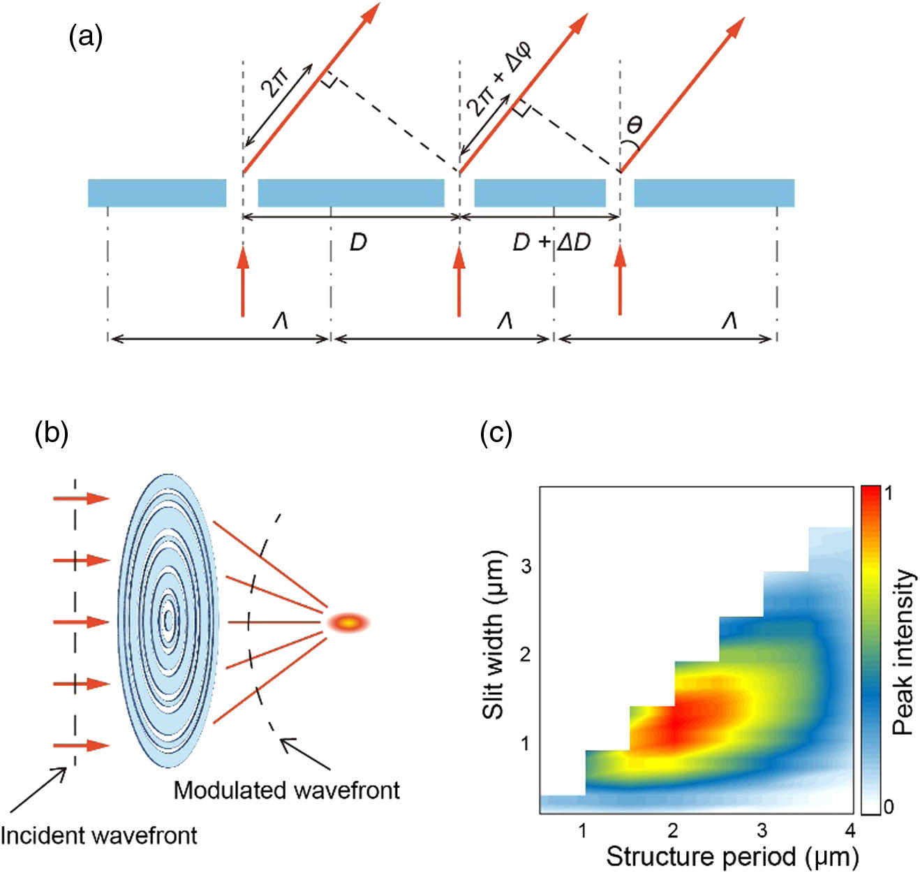
    Fig. 1. PUP lens design based on the detour phase method. (a) Schematic illustration of the detour phase modulation rule for arbitrary wavefront shaping. (b) Focusing from the constructive interference of wavelets by the PUP lens. (c) Peak intensity of the focus with respect to structure periods and slit widths.
    Direct laser writing of PUP lenses on perovskite films. (a) Schematic illustration of the femtosecond laser fabrication process of PUP lenses. (b) Theoretically calculated lens profile with concentric rings. Scale bar: 10 μm. (c) Fabricated PUP lens imaged by a wide-field optical microscope. Scale bar: 10 μm. (d) Fluorescence image of the fabricated PUP lens. Scale bar: 10 μm. (e) AFM image of a region of the fabricated PUP lens and the corresponding height profile along the white dashed line. Scale bar: 4 μm.
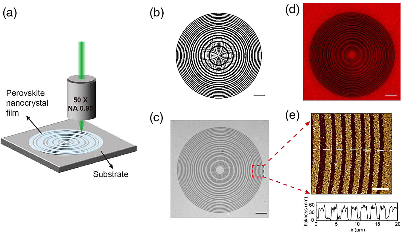
    Fig. 2. Direct laser writing of PUP lenses on perovskite films. (a) Schematic illustration of the femtosecond laser fabrication process of PUP lenses. (b) Theoretically calculated lens profile with concentric rings. Scale bar: 10 μm. (c) Fabricated PUP lens imaged by a wide-field optical microscope. Scale bar: 10 μm. (d) Fluorescence image of the fabricated PUP lens. Scale bar: 10 μm. (e) AFM image of a region of the fabricated PUP lens and the corresponding height profile along the white dashed line. Scale bar: 4 μm.
    Calculated and measured focus fields. (a) Calculated lateral (left) and axial (right) focusing intensity distributions of the designed PUP lens. (b) Measured lateral (left) and axial (right) focusing intensity distributions of the fabricated PUP lens. (c) The calculated (red) and measured (blue) cross-sectional intensity distributions (normalized) of the focal spot along the lateral direction (left) and axial direction (right). (d) Measured 3D focusing intensity distribution near the focal spot. (e) Experimental setup to characterize the focusing intensity distributions of the PUP lenses.
    Fig. 3. Calculated and measured focus fields. (a) Calculated lateral (left) and axial (right) focusing intensity distributions of the designed PUP lens. (b) Measured lateral (left) and axial (right) focusing intensity distributions of the fabricated PUP lens. (c) The calculated (red) and measured (blue) cross-sectional intensity distributions (normalized) of the focal spot along the lateral direction (left) and axial direction (right). (d) Measured 3D focusing intensity distribution near the focal spot. (e) Experimental setup to characterize the focusing intensity distributions of the PUP lenses.
    Focusing characterization with PUP lenses fabricated under different laser power. (a) In-plane images at focal plane with different laser power. All intensity values are normalized to the respective peak intensity. Scale bar: 2 μm. (b) Calculated (red) and measured (blue) peak intensity of the focal spot with lenses fabricated under different laser power. (c) Ablated linewidth of the concentric rings with lenses fabricated under different laser power. (d) FWHM of the focal spot along the lateral (blue) and axial (red) directions with lenses fabricated under different laser power. All error bars were created by the standard deviations of datapoints under three measurements.
    Fig. 4. Focusing characterization with PUP lenses fabricated under different laser power. (a) In-plane images at focal plane with different laser power. All intensity values are normalized to the respective peak intensity. Scale bar: 2 μm. (b) Calculated (red) and measured (blue) peak intensity of the focal spot with lenses fabricated under different laser power. (c) Ablated linewidth of the concentric rings with lenses fabricated under different laser power. (d) FWHM of the focal spot along the lateral (blue) and axial (red) directions with lenses fabricated under different laser power. All error bars were created by the standard deviations of datapoints under three measurements.
    Imaging using a PUP lens. (a) Direct imaging of the characters from a 1951 USAF resolution test target using the homemade optical microscopy imaging system. Scale bar: 20 μm. (b) Imaging of the characters from the 1951 USAF resolution test target using a PUP lens. Scale bar: 5 μm. (c) and (d) Imaging of the characters and lines from the 1951 USAF resolution test target using a perovskite planar lens with the addition of PMMA. Scale bar: 5 μm.
    Fig. 5. Imaging using a PUP lens. (a) Direct imaging of the characters from a 1951 USAF resolution test target using the homemade optical microscopy imaging system. Scale bar: 20 μm. (b) Imaging of the characters from the 1951 USAF resolution test target using a PUP lens. Scale bar: 5 μm. (c) and (d) Imaging of the characters and lines from the 1951 USAF resolution test target using a perovskite planar lens with the addition of PMMA. Scale bar: 5 μm.
    Characteristics of the perovskite nanocrystal film. (a) Transmission electron microscope (TEM) image of the perovskite nanocrystals. The nanocrystal sizes were calculated manually using "Nano Measurer" software (Nano Measurer 1.2, https://nano-measurer.software.informer.com/). Scalar bar: 100 nm. (b) Raman spectrum of the perovskite nanocrystal film. (c) Fluorescence spectrum of the perovskite nanocrystal film. (d) Transmittance spectrum of the perovskite nanocrystal film.
    Fig. 6. Characteristics of the perovskite nanocrystal film. (a) Transmission electron microscope (TEM) image of the perovskite nanocrystals. The nanocrystal sizes were calculated manually using "Nano Measurer" software (Nano Measurer 1.2, https://nano-measurer.software.informer.com/). Scalar bar: 100 nm. (b) Raman spectrum of the perovskite nanocrystal film. (c) Fluorescence spectrum of the perovskite nanocrystal film. (d) Transmittance spectrum of the perovskite nanocrystal film.
    AFM images and corresponding height profiles of the PUP lenses fabricated with laser power ranging from 10 mW to 35 mW.
    Fig. 7. AFM images and corresponding height profiles of the PUP lenses fabricated with laser power ranging from 10 mW to 35 mW.
    Imaging of the 1951 USAF resolution test target using the homemade microscope imaging system. Scale bar: 200 μm.
    Fig. 8. Imaging of the 1951 USAF resolution test target using the homemade microscope imaging system. Scale bar: 200 μm.
    Element distribution measurement of the laser scribed perovskite nanocrystal film. (a) Femtosecond laser scribed region imaged by SEM. (b) In-situ element distribution measurement on the same region as (a). Scale bar: 5 μm.
    Fig. 9. Element distribution measurement of the laser scribed perovskite nanocrystal film. (a) Femtosecond laser scribed region imaged by SEM. (b) In-situ element distribution measurement on the same region as (a). Scale bar: 5 μm.
    Wenkai Yang, Lige Liu, Dashan Dong, Xin Zhang, Han Lin, Yunkun Wang, Hong Yang, Yunan Gao, Haizheng Zhong, Baohua Jia, Kebin Shi. Detour-phased perovskite ultrathin planar lens using direct femtosecond laser writing[J]. Photonics Research, 2022, 10(12): 2768
    Download Citation