Wenkai Yang1,2,†, Lige Liu1,2,†, Dashan Dong1,2, Xin Zhang3..., Han Lin4, Yunkun Wang1,2, Hong Yang1,2, Yunan Gao1,2, Haizheng Zhong3, Baohua Jia4 and Kebin Shi1,2,5,*|Show fewer author(s)
1State Key Laboratory for Mesoscopic Physics and Frontiers Science Center for Nano-optoelectronics, School of Physics, Peking University, Beijing 100871, China
2Collaborative Innovation Center of Extreme Optics, Shanxi University, Taiyuan 030006, China
3MIIT Key Laboratory for Low-Dimensional Quantum Structure and Devices, School of Materials Sciences and Engineering, Beijing Institute of Technology, Beijing 100081, China
4School of Science, RMIT University, Melbourne 3000, VIC, Australia
5Peking University Yangtze Delta Institute of Optoelectronics, Nantong 226010, China
Perovskite-enabled optical devices have drawn intensive interest and have been considered promising candidates for integrated optoelectronic systems. As one of the important photonic functions, optical phase modulation previously was demonstrated with perovskite substrate and complex refractive index engineering with laser scribing. Here we report on the new scheme of achieving efficient phase modulation by combining detour phase design with 40 nm ultrathin perovskite films composed of nanosized crystalline particles. Phase modulation was realized by binary amplitude patterning, which significantly simplifies the fabrication process. Perovskite nanocrystal films exhibit significantly weak ion migration effects under femtosecond laser writing, resulting in smooth edges along the laser ablated area and high diffractive optical quality. Fabrication of a detour-phased perovskite ultrathin planar lens with a diameter of 150 μm using femtosecond laser scribing was experimentally demonstrated. A high-performance 3D focus was observed, and the fabrication showed a high tolerance with different laser writing powers. Furthermore, the high-quality imaging capability of perovskite ultrathin planar lenses with a suppressed background was also demonstrated.
1. INTRODUCTION
Optical lenses are indispensable elements in modern scientific research and industrial applications due to their distinctive focusing and imaging capabilities [1–3]. Focusing is the result of a specific wavefront modulation after a light wave passes through the lens plane. The wavefront modulation in a conventional optical lens is from phase accumulation depending on the lens thickness and the refractive index difference between the lens and the surrounding medium. Due to the limited refractive index of naturally available transparent materials, it is fundamentally impossible to achieve diffraction-limited focusing using conventional optical lenses with subwavelength thicknesses, making conventional optical lenses bulky and hindering their integration into compact, cost-effective systems.
One way to deal with this challenge is to use planar lenses, such as metalenses [4,5], and conventional diffractive lenses including super-oscillatory lenses [6,7], supercritical lenses [8], and low-dimension, material-based lenses [9,10]. These lenses can be suitably integrated into a variety of nano-optics and on-chip photonic systems, as well as portable and wearable optical devices and systems due to their distinctive advantages of nanometer thickness, ultralight weight, and flat structure [11]. In a metalens, the phase is induced via the response of the subwavelength quasi-periodic structure built on the surface of a substrate. However, the fabrication of complicated nanostructures requires expensive and sophisticated multistep processes, including electron beam lithography, or a large-scale semiconductor fabrication facility [12]. Conventional planar diffractive lenses, which are primarily zone-plate-based lenses, can be designed and fabricated with larger constituent features, making it possible to use low-cost and large-scale manufacturing techniques [13], particularly the mask-free direct laser writing (DLW) process, which opens up new possibilities to enable high-performance optical elements and devices [9,14–17]. The zone-plate-based lenses, especially graphene oxide (GO) lenses, can achieve highly efficient 3D focusing with high resolution by using phase and amplitude modulation simultaneously with 200 nm thickness [9,10,18]. However, further reducing the thickness of GO will compromise the focusing efficiency and resolution due to the limited phase accumulations. Recently, Lin et al. reported on the use of 2D materials ( in thickness) to achieve 3D focusing with subwavelength resolution [19], but this was achieved mainly by relying on the large refractive index (5.5 at 633 nm) of a monolayer .
Perovskites are promising candidates for applications in lasers, LEDs, solar cells, and patterning due to their excellent optical and electronic properties [20]. The advantage of in situ synthesis of perovskite materials from a precursor solution facilitates the low-cost fabrication of the optoelectronic devices [21]. Furthermore, extremely low thermal conductivity () and the high defect tolerance of the perovskites compared with other materials [22] such as graphene-based materials () [23], protect the surrounding morphology from severe damage by light-induced overheating and make precise spatial control easily attainable during laser processing. Recently, femtosecond DLW has been used in perovskites to pattern microstructures and fabricate optical devices [22,24,25]. A zone-plate-based thin film perovskite planar lens was previously reported [26], where the design was limited to a small aperture of μ because the widths of the edge zones in a zone-plate-design become extremely narrow (sub-wavelength scale) and hard to implement by direct laser writing. Furthermore, the use of single-crystalline perovskite nanosheets will inevitably suffer from phase separation, particularly in mixed halide perovskite due to laser-induced ion migration outside the ablated area, which will significantly change the uniformity of ion distributions as well as the material characteristics such as transmittance, refractive index, and absorptivity throughout the surface [25,27], making it difficult in a zone-plate-based design to precisely control the modulated electronic fields for the lenses relying on both amplitude and phase modulation.
Sign up for Photonics Research TOC. Get the latest issue of Photonics Research delivered right to you!Sign up now
Here, we report on the theoretical design and experimental fabrication of high-performance perovskite nanocrystal ultrathin planar (PUP) lenses with a thickness of 40 nm and a diameter of 150 μm based on the detour phase method. Unlike zone-plate-based lenses, the linewidth can be selected flexibly regardless of the focal length in the detour phase method. The use of the detour phase with amplitude-only modulation and the femtosecond laser direct writing technique with one-step mask-free ablation greatly simplified lens design and manufacture. Moreover, perovskite films composed of nanosized crystalline particles exhibit significantly weak ion migration effects due to the reduced carrier diffusion lengths in contrast to the microsized single crystal and polymorphs bulk perovskite films [28,29], resulting in smooth edges along the ablated area and uniform morphology throughout the films. A uniform ion distribution was observed in the laser scribed sample by the element distribution measurement (as shown and discussed in Fig. 9 in Appendix E), which indicates the ion migration during the laser scribing is negligible. A theoretical model is presented to investigate the focus field based on the scalar Fresnel diffraction theory. A high-performance 3D focus was observed and the fabrications with different parameters were investigated. Finally, the imaging capability of the PUP lenses was also demonstrated.
2. RESULTS AND DISCUSSION
A. Lens Design Based on Detour Phase Method
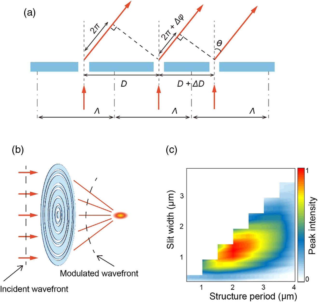
The design of PUP lenses in this study originates from detour phase holography, which was first proposed by Brown and Lohmann [30]. It is a very convenient approach to control light within a single ultrathin interface. A detour phase hologram is particularly intriguing since it achieves 2D phase modulation using binary amplitude-only holograms based on the positions and sizes of an array of transmitted apertures on an opaque screen. This method has been widely used to design the aperture distributions in computer-generated holography [31–33], and it has recently been extended to fields such as meta-holograms [34–36], nonlinear holography [37,38], and beam shaping [39–41]. Because the phase profile of a lens is circularly symmetric, we only consider aperture distributions along the radial direction so that the design of detour phase holograms can be simplified to one dimension. The principle of the phase modulation of the PUP lens is depicted in Fig. 1(a). A grating with a period of and three slits with varying center-to-center distances is used for illustration. When a light beam is incident on the grating, it is diffracted at each slit, producing a second wave. The center-to-center distance () between the first two slits equals the structure period (), resulting in diffracted light from these two slits being in-phase along a given direction () if , where is the working wavelength. However, if the third slit is slightly out of position by a distance of in a period, the emerging wavefront will diffract differently. The third slit and the second slit will no longer be in-phase along the given direction (), and the phase difference between them depends on their distance. This indicates that the desired phase shift between two adjacent slits can be obtained by shifting the spatial position:
Figure 1.PUP lens design based on the detour phase method. (a) Schematic illustration of the detour phase modulation rule for arbitrary wavefront shaping. (b) Focusing from the constructive interference of wavelets by the PUP lens. (c) Peak intensity of the focus with respect to structure periods and slit widths.
When the slit shift () varies from 0 to in each period, a phase shift between the adjacent slits covering the range from to is obtained, allowing for a versatile method of phase modulation. Furthermore, one can also conclude from Eq. (1) that to achieve the complete range of phase modulation, the available position shift range of the slit should be larger than the working wavelength (), because the maximum diffraction angle () is 90°. The phase modulation induced by detour phase method also can be understood as follows. The phase change in the spatial frequency is the Fourier transform of the position shift in the space domain. To design the perovskite planar lens, the parabolic phase profile of a convergence lens is considered, which is given by the phase function [42]where is the radial coordinate and is the designed focal length of the lens. The phase profile in Eq. (2) can then be discretized by repeating the structure period along the radial direction and adjusting the slit shift in each period. The center position of the th slit will be given as . Finally, the lens profile based on the detour phase method can be digitally recorded at the lens plane by rotating the grating perpendicular to the radial direction. The focusing is a result of the constructive interference of wavelets originated in the lens plane from different slits, as depicted in Fig. 1(b).
The structure period and slit width are both critical in lens design because they affect the sampling resolution of the phase profile, the overall power of the transmitted light, and the phase modulation coverage. Moreover, the lens design will be impracticable if the minimum achievable linewidth, determined by the spot size of the diffraction limited focal spot in the DLW process, is larger than the designed slit width. To find out the optimal parameters to facilitate the lens performance, the influence of the structure period and slit width on the focus intensity was first investigated. A PUP lens with a working wavelength of 532 nm, a focal length () of 310 μm, and a lens radius () of 75 μm was designed. The resulting NA of the lens is 0.24 from , and the intensity distribution in the focal region of the PUP lens was calculated using the Fresnel scalar diffraction theory [43]. Figure 1(c) shows the variations in peak intensity of the focal spot with respect to structure periods and slit widths. No data was generated in the white area because the slit width should not exceed the structure period. The highest peak intensity of the focus was obtained when the structure period is 2 μm and the slit width is around 1 μm with a calculated focusing efficiency of around 16%. The focusing efficiency is defined as the fraction of light passing through a circular iris with a radius three times the FWHM spot size in the focal plane [44]. For a fixed slit width, the drop in peak intensity at other periods is mainly due to insufficient sampling at larger periods, and insufficient phase modulation coverage at smaller periods at the designed working wavelength. Peak intensity varies at different slit widths for a given structure period because a smaller slit width leads to finer phase modulation but reduces the overall transmitted light, whereas a larger slit width causes crosstalk and limits the available slit shift range, making phase modulation insufficient to cover the complete range from to . A tradeoff between the overall transmitted light and phase modulation coverage results in the highest peak intensity being found when the slit width is around half the structure period. It should be noted that changing the focal length or radius of the lens will make the results diverge from this design. Overall, the technique based on the detour phase method provides a versatile method for lens design. The width of the slit and the period of the structure can be varied flexibly to satisfy specific requirements in practical applications, and the NA of the lens can be modified simply by changing the number of slits.
B. Fabrication of PUP Lenses
The PUP lens was fabricated by a direct femtosecond laser writing process, as illustrated in Fig. 2(a), and the transparent slits were produced by laser ablation of perovskite nanocrystal films. The perovskite nanocrystal films were prepared by spin-coating the precursor solution onto a glass substrate following the method used by Zhang et al. [45]. The mean size of the nanocrystals was measured by the transmission electron microscope (TEM) image [Fig. 6(a) in Appendix A] and the perovskite was an [formamidine lead iodide, ] phase as revealed by Raman spectrum [Fig. 6(b) in Appendix A] [46,47]. A green femtosecond laser source, which operates at 515 nm with a pulse repetition rate of 55 MHz and a pulse width of 120 fs, was generated via the second harmonic generation process from a homemade Yb-doped femtosecond fiber laser. The average power of the femtosecond laser pulses was set to 25 mW and was focused onto perovskite nanocrystal films using an objective lens with a magnification of 50 and an NA of 0.95. A high-precision, two-axis translation stage was used to move the sample at a scanning speed of 20 μm/s in the writing process. A PUP lens with a working wavelength of 532 nm, focal length of 310 μm, and a diameter of 150 μm was designed. To optimize the lens focusing performance, the structure period was set to 2 μm and the linewidth was set to 1 μm based on the calculation results from the previous discussion. The calculated lens profile consisting of concentric rings is shown in Fig. 2(b). The fixed linewidth of the transparent rings distinguishes the detour phase design from the traditional Fresnel zone plate, in which the width of the alternate transparent and opaque zones decreases farther from the center. The width of the zones becomes extremely narrow and the density of the zones becomes very high at the edge of Fresnel zone plate, making it challenging to fabricate large aperture planar lenses. The fabricated perovskite lens imaged by a wide-field optical microscope is shown in Fig. 2(c). The innermost three rings were deliberately eliminated during the fabrication due to the limited minimum incremental motion of the stage () and were confirmed to have a negligible impact on the focus performance. Figure 2(d) shows a fluorescence image of the PUP lens under the illumination of a mercury lamp. The red background represents the fluorescence emitted from perovskites with a central wavelength of [Fig. 6(c) in Appendix A] and the fluorescence was not detected in the ablated concentric rings. The emitted fluorescence does not affect the focusing performance since it is incoherent and will not interfere with the transmitted light from illumination laser [26]. The formation of the ablated rings was confirmed by an atomic force microscope (AFM) image of a region of the fabricated PUP lens, as shown in Fig. 2(e). The linewidth of the rings is μ and the thickness of the perovskite film is , as presented in the corresponding height profile along the white dashed line. The desired lens profile is produced in a single-step writing process without any back-and-forth optimization, showing the significant benefits of the one-step mask-free DLW technique. Perovskites have significantly lower thermal conductivity [22] compared to other materials frequently used in the production of ultrathin planar lenses. Graphene oxide [9], for example, has high thermal conductivity and is sensitive to the heat accumulation during the writing process [23], which requires the use of expensive, low repetition rate laser pulses at the kHz level. The structure patterned on perovskite film by the 55 MHz femtosecond laser pulses exhibits high-quality morphology along the writing edge, which is advantageous in using the much cheaper high-repetition-rate femtosecond lasers. The standard deviation of the surface roughness at the unprocessed area is 4.06 nm (10.15%, considering the lens thickness of 40 nm). The surface roughness will affect the lens performance to some extent, which can be improved with the development of nanocrystal film preparation technology.
Figure 2.Direct laser writing of PUP lenses on perovskite films. (a) Schematic illustration of the femtosecond laser fabrication process of PUP lenses. (b) Theoretically calculated lens profile with concentric rings. Scale bar: 10 μm. (c) Fabricated PUP lens imaged by a wide-field optical microscope. Scale bar: 10 μm. (d) Fluorescence image of the fabricated PUP lens. Scale bar: 10 μm. (e) AFM image of a region of the fabricated PUP lens and the corresponding height profile along the white dashed line. Scale bar: 4 μm.
The detour phase technique has the benefit of considering only the amplitude modulation generated by the position shift of the concentric rings in the perovskite lens plane. As a result, the light field behind the lens was the product of the incident light field and the transmittance of the lens. Considering the NA of 0.24 for the designed PUP lens, it is feasible to calculate the intensity distribution near the focal spot using paraxial approximation. Figure 3(a) is the calculated intensity distribution around the focal spot based on the Fresnel scalar diffraction theory under 532 nm plane wave illumination. Well-defined strong focus from both the lateral and axial directions with ignorable side lobes ( of the peak intensity) is achieved. The corresponding cross-sectional plots along the lateral direction and axial direction are shown in Fig. 3(c). The calculated FWHM of the focal spot in the lateral direction is 1.01 μm (left, red solid line), while in the axial direction (right, red solid line) is 14.92 μm. A laser diode with a wavelength of 532 nm was used to characterize the focusing intensity distribution of the PUP lens. The experimental setup is depicted in Fig. 3(e) and more details can be found in Appendix C. To acquire a uniform intensity, the diameter of the beam from the laser diode was expanded to around 1 cm before entering the lens. To obtain the 3D focal spot, a motorized linear stage was used to move the objective (, ) along the optical axis with a step size of 100 nm. In-plane images of the intensity distributions behind the lens in the axial direction were recorded by a CMOS camera after each step of moving, and the volume view of the focal spot was obtained by stacking all the in-plane images. The focal length was measured by calculating the stage traveling distance when the lens plane and the focal spot were clearly imaged successively. The measured focusing intensity distribution along the lateral direction and axial direction are shown in Fig. 3(b), and the corresponding cross-sectional plots are shown in Fig. 3(c). The measured FWHM of the focal spot in the lateral direction is 1.07 μm (left, blue dotted line) while in axial direction is 14.75 μm (right, blue dotted line), leading to a high-quality 3D focal spot, as shown in Fig. 3(d). The experimental results show good agreement with the theoretical calculation. The slight difference in focal spot size in the axial direction could be attributed to the limited minimum incremental motion (100 nm) of the motorized linear stage, the imperfection of the fabrication, and the surface roughness of the perovskite film. The deviation in focal length between the theoretical calculation (302 μm) and experimental measurements (297 μm) is only 1.7%, indicating a high reliability of the theoretical design to guide the practical experiments.
Figure 3.Calculated and measured focus fields. (a) Calculated lateral (left) and axial (right) focusing intensity distributions of the designed PUP lens. (b) Measured lateral (left) and axial (right) focusing intensity distributions of the fabricated PUP lens. (c) The calculated (red) and measured (blue) cross-sectional intensity distributions (normalized) of the focal spot along the lateral direction (left) and axial direction (right). (d) Measured 3D focusing intensity distribution near the focal spot. (e) Experimental setup to characterize the focusing intensity distributions of the PUP lenses.
To further evaluate the tolerance of the lens fabrication throughout the DLW process, the focusing performance of six lenses fabricated under different laser power ranging from 10 to 35 mW is presented in Fig. 4. The minimum average power required to induce ablation on the surface of the perovskite film was 10 mW, resulting in an ablation depth of with a rugged morphology along the edge of the concentric ring confirmed by AFM measurement [Fig. 7(a) in Appendix B]. The SNR of the peak intensity of the focal spot to background at the focal plane is [or 11% of the peak intensity of the lens fabricated at 35 mW, as shown in Fig. 4(b)]. When the average power of the femtosecond laser pulses reaches 15 mW, the ablation area penetrates the whole film to a depth of [Figs. 7(b)–7(f) in Appendix B]. The focal spots show outstanding quality and the focusing intensity grows accordingly as the laser power varies from 15 to 35 mW, as shown in Figs. 4(a) and 4(b), respectively. The experimental measurements agree well with the calculations in the power dependency, as depicted by the blue and red dotted lines in Fig. 4(b). The linewidth grows linearly with an increase in the laser power, as presented in Fig. 4(c), indicating that the linewidth can be flexibly tuned by simply changing the laser power, which provides a convenient way to meet the requirements for different lens designs. It is interesting to find that although the peak intensity of the focal spots and the linewidth of the concentric rings vary according to the laser power, the FWHMs of the focal spots in the lateral and axial directions remain nearly constant, except for the one imperfectly fabricated at 10 mW, as shown in Fig. 4(d). This also implies a significant advantage of the high-fidelity fabrication of planar lenses using perovskite films.
Figure 4.Focusing characterization with PUP lenses fabricated under different laser power. (a) In-plane images at focal plane with different laser power. All intensity values are normalized to the respective peak intensity. Scale bar: 2 μm. (b) Calculated (red) and measured (blue) peak intensity of the focal spot with lenses fabricated under different laser power. (c) Ablated linewidth of the concentric rings with lenses fabricated under different laser power. (d) FWHM of the focal spot along the lateral (blue) and axial (red) directions with lenses fabricated under different laser power. All error bars were created by the standard deviations of datapoints under three measurements.
To demonstrate the imaging capability of a PUP lens, we performed an imaging test using a 1951 USAF resolution test target. The target was placed in front of the PUP lens and the images were further magnified using the previously mentioned homemade microscope imaging system [Fig. 3(e)]. Figure 5(a) shows the images taken directly by the homemade microscope imaging system, and the interference fringes occur due to coherent illumination using the 532 nm laser diode. The PUP lens used here was fabricated with an average laser power of 25 mW and a scanning speed of 20 μm/s. The minimum objective distance accessible due to system limitations is 3270.3 μm; therefore, the characters from 1 to 6 were captured at an image distance of 326.2 μm, as shown in Fig. 5(b). The calculated focal length according to the lens equation is 296.6 μm, which is in good agreement with the measured one of around 297 μm. Furthermore, the size of the characters in Fig. 5(b) is one tenth of size of the characters in Fig. 5(a), leading to a magnification of , which is also in good agreement with the calculated one by dividing the image distance with the objective distance. It is noticed that moderate background noise exists and decreases the SNR in Fig. 5(b), which originates from the defocused patterns on the test target that penetrated the lens plane due to the high transmittance [, Fig. 6(d) in Appendix A] of the ultrathin perovskite film. Subsequently, we prepared another perovskite film by adding the polymer known as polymethyl methacrylate (PMMA) into the precursor solution to further illustrate the imaging capability of the perovskite lenses, and the imaging results from the test target are presented in Figs. 5(c) and 5(d). The preparation method of the precursor solution can be found in our previous work [48]. The addition of PMMA not only reduces the transmittance of the films but also improves the environmental stability of perovskites [49]. The contrast and the SNR of the images are both improved, as shown in Fig. 5(c) due to the suppression of the background transmission. Another reason for the imperfect imaging quality is the use of coherent illumination. To further improve the image quality, an incoherent light source could be used for illumination.
Figure 5.Imaging using a PUP lens. (a) Direct imaging of the characters from a 1951 USAF resolution test target using the homemade optical microscopy imaging system. Scale bar: 20 μm. (b) Imaging of the characters from the 1951 USAF resolution test target using a PUP lens. Scale bar: 5 μm. (c) and (d) Imaging of the characters and lines from the 1951 USAF resolution test target using a perovskite planar lens with the addition of PMMA. Scale bar: 5 μm.
In conclusion, we have reported on the theoretical design and experimental fabrication of high-performance perovskite ultrathin planar lenses with a thickness of 40 nm based on the detour phase method. The ablated area of the perovskite nanocrystal films showed smooth edges using a one-step, mask-free femtosecond laser direct writing technique. A theoretical model was presented to investigate the focus field based on the scalar Fresnel diffraction theory and matched well with the experimental results. High-performance 3D focus was observed and the fabrication showed high tolerance with different laser writing powers. Furthermore, the high-quality imaging capability of the PUP lenses with a suppressed background was also demonstrated. We believe the low-cost in situ preparation of perovskite materials together with the fabrication of high-performance PUP lenses using the DLW technique opens new avenues for broad photonic applications and miniaturized on-chip devices.
Acknowledgment
Acknowledgment. The authors acknowledge support from the High Performance Computing Facility of Peking University.
APPENDIX A: PREPARATION AND CHARACTERISTICS OF PEROVSKITE FILMS
The perovskite nanocrystal films were prepared by spin-coating the precursor solution onto the glass substrate. The precursor solutions were made by dissolving formamidinium iodide (FAI, 68.8 mg), (lead iodide, 184.4 mg), and DPPA-Br (3,3-diphenylpropylamine bromide, 46.8 mg) in 2 mL DMF (N,N-dimethylformamide), and then stirred for 2 h at 60°C in a glove box. The precursor solution (200 μL) was dropped on the substrate after being filtered through a 0.45 μm organic nylon filter and spin-coated onto the substrate for 60 s at 8000 r/min. The resultant samples were annealed at 100°C for 5 min to form the perovskite nanocrystal films. The optical properties of the perovskite nanocrystal films are presented in Fig. 6.
Figure 6.Characteristics of the perovskite nanocrystal film. (a) Transmission electron microscope (TEM) image of the perovskite nanocrystals. The nanocrystal sizes were calculated manually using "Nano Measurer" software (Nano Measurer 1.2, https://nano-measurer.software.informer.com/). Scalar bar: 100 nm. (b) Raman spectrum of the perovskite nanocrystal film. (c) Fluorescence spectrum of the perovskite nanocrystal film. (d) Transmittance spectrum of the perovskite nanocrystal film.
APPENDIX B: AFM CHARACTERIZATION OF PUP LENSES FABRICATED WITH DIFFERENT LASER POWERS
Six PUP lenses were fabricated to investigate the power dependence as well as the fabrication tolerance with the laser power ranging from 10 mW to 35 mW. The scanning speed of the stage was set to 20 μm/s. The AFM images of the six PUP lenses and the corresponding height profiles along the cross sections are presented in Fig. 7.
Figure 7.AFM images and corresponding height profiles of the PUP lenses fabricated with laser power ranging from 10 mW to 35 mW.
The PUP lens characterization was performed with a homemade microscope imaging system, as schematically illustrated in Fig. 3(e). The diameter of the beam from a 532 nm laser diode was collimated and expanded to around 1 cm before entering the lens to acquire a uniform intensity. A high NA objective (, ) was mounted on a motorized linear stage (combination of an LTA-HS high speed motorized actuator and an M-423 linear translation stage from Newport) to record the in-plane images at different distances along the optical axis. A CMOS camera (MC050MG-SY, XIMEA) was used to record the in-plane images.
APPENDIX D: DEMONSTRATION OF IMAGING CAPABILITY USING A TEST TARGET
We used a negative 1951 USAF resolution test target (R1DS1N, Thorlabs) to demonstrate the imaging capability of the PUP lens, which consists of a chrome coating to cover the substrate with the pattern to be transparent, and is suitable in back-lit and highly illuminated applications. Figure 8 presents a portion of the target imaged by the homemade microscope imaging system (with a objective lens). The target consists of six groups and the group number will specify the size category. Each element has a set resolution based on which group the element belongs to while the numbers in the same group have the same size. We chose group four in the experiment, considering the field of view of the PUP lens.
Figure 8.Imaging of the 1951 USAF resolution test target using the homemade microscope imaging system. Scale bar: 200 μm.
APPENDIX E: MEASUREMENT OF ION MIGRATION EFFECT ON PEROVSKITE NANOCRYSTAL FILM SCRIBED BY FEMTOSECOND LASER
Element distribution measurement was performed using a field emission scanning electron microscope (Hitachi FE-SEM S-4800 with Horiba EDX system). The SEM image of the laser scribed perovskite nanocrystal film (spin-coated on a silicon substrate) is shown in Fig. 9(a). The in-situ element distribution measurement was performed simultaneously on the same sample and is shown in Fig. 9(b), where the uniform elements distribution can be observed.
Figure 9.Element distribution measurement of the laser scribed perovskite nanocrystal film. (a) Femtosecond laser scribed region imaged by SEM. (b) In-situ element distribution measurement on the same region as (a). Scale bar: 5 μm.