Yuting Ye, Hui Ma, Chunlei Sun, Zequn Chen, Jianghong Wu, Yiqi Chen, Ye Luo, Hongtao Lin, Lan Li. Research Progress on Flexible Photonic Materials and Devices[J]. Laser & Optoelectronics Progress, 2020, 57(3): 030001
Search by keywords or author
- Laser & Optoelectronics Progress
- Vol. 57, Issue 3, 030001 (2020)
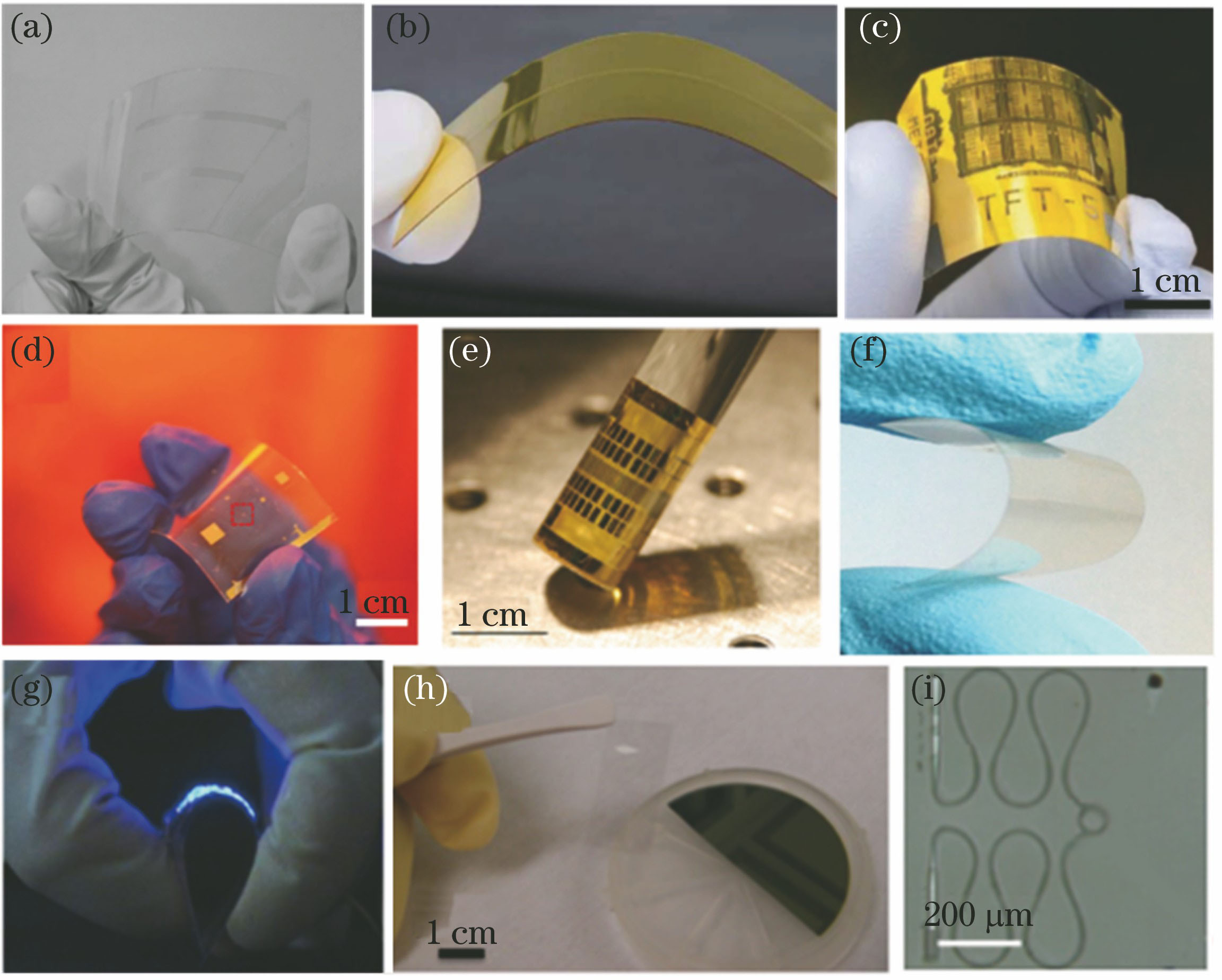
![Flexible photonic devices based on different materials. (a) Flexible polymer waveguide cladded in PDMS[25]; (b) flexible optical waveguide cladded in PI[26]; (c) flexible Si NM phototransistor[34]; (d) array of Ge NM MSM photodiodes on PET substrate[75]; (e) 8 × 100 thin-film InGaAs p-i-n photodiode](/richHtml/lop/2020/57/3/030001/img_1.jpg)
Fig. 1. Flexible photonic devices based on different materials. (a) Flexible polymer waveguide cladded in PDMS[25]; (b) flexible optical waveguide cladded in PI[26]; (c) flexible Si NM phototransistor[34]; (d) array of Ge NM MSM photodiodes on PET substrate[75]; (e) 8 × 100 thin-film InGaAs p-i-n photodiode
![Design of multi-neutral plane structure. (a) Pure bending of multi-layer structure, whose top and bottom surfaces undergo tensile and compressive strain, respectively. The neutral plane position is specified by Equation (1)[85]; (b) finite element simulation results of strain distribution in two thin-film structures with bending radius of 1 mm. The blue curve corresponds to strain in a polyimide (10 μm)-silicone (50 μm)-polyimide (10 μm) tri-laye](/richHtml/lop/2020/57/3/030001/img_2.jpg)
Fig. 2. Design of multi-neutral plane structure. (a) Pure bending of multi-layer structure, whose top and bottom surfaces undergo tensile and compressive strain, respectively. The neutral plane position is specified by Equation (1)[85]; (b) finite element simulation results of strain distribution in two thin-film structures with bending radius of 1 mm. The blue curve corresponds to strain in a polyimide (10 μm)-silicone (50 μm)-polyimide (10 μm) tri-laye
Fig. 3. Meandering and isolated structure based stretchable devices. (a) Procedures for the fabrication of honeycomb metamaterial with wrinkled layouts[91]; (b) schematic of integrated stretchable photonic device based on the design of meandering waveguide and local hardening[96]; (c) optical micrographs of waveguide coupled microring resonator without tensile strain and with 36% tensile strain[![General process illustration for semiconductor membrane release, transfer, and stacking[85]](/Images/icon/loading.gif)
![Fabrication process of monolithic integration of flexible photonic devices[87]](/Images/icon/loading.gif)
![Hybrid integration technology for flexible photonic devices. (a) Schematic of fabrication process of flexible waveguide-integrated detector[88]; (b) optical micrograph of flexible waveguide integrated detector[88]](/Images/icon/loading.gif)
![Applications of flexible photonic devices in sensing field. (a) Flexible fibers for monitoring knees' weight bearing[127]; (b) eye pressure sensor based on deformation of periodically nanostructured Bragg grating[126]; (c) stretchable optical waveguides based on soft robotic hand for optoelectronic strain sensing[123]; (d) polymer waveguide base](/Images/icon/loading.gif)
![Flexible photonic devices for optical interconnect. (a) Diagram and (b) photo of flexible optical interconnection scheme using fully embedded optical link with polymer waveguides, mirrors, and optoelectronic components[151];(c) stretchable optical link including integrated light sources, detectors, and polymer waveguide[146]; (d) schematic of high-density integration optical interconnect based o](/Images/icon/loading.gif)
![Applications of flexible photonic devices in new optical field manipulation. (a) Continuous reconfigurable switching of multiple holograms based on stretchable metasurface structure[156]; (b) flexible Bragg grating based tunable organic DFB lasers[158]; (c) schematic of dielectric metasurface layer conformed to the surface of transparent object with arbitrary geometry[<xref ref-type="bibr"](/Images/icon/loading.gif)
Fig. 4. General process illustration for semiconductor membrane release, transfer, and stacking[85]
Fig. 5. Fabrication process of monolithic integration of flexible photonic devices[87]
Fig. 6. Hybrid integration technology for flexible photonic devices. (a) Schematic of fabrication process of flexible waveguide-integrated detector[88]; (b) optical micrograph of flexible waveguide integrated detector[88]
Fig. 7. Applications of flexible photonic devices in sensing field. (a) Flexible fibers for monitoring knees' weight bearing[127]; (b) eye pressure sensor based on deformation of periodically nanostructured Bragg grating[126]; (c) stretchable optical waveguides based on soft robotic hand for optoelectronic strain sensing[123]; (d) polymer waveguide base
Fig. 8. Flexible photonic devices for optical interconnect. (a) Diagram and (b) photo of flexible optical interconnection scheme using fully embedded optical link with polymer waveguides, mirrors, and optoelectronic components[151];(c) stretchable optical link including integrated light sources, detectors, and polymer waveguide[146]; (d) schematic of high-density integration optical interconnect based o
Fig. 9. Applications of flexible photonic devices in new optical field manipulation. (a) Continuous reconfigurable switching of multiple holograms based on stretchable metasurface structure[156]; (b) flexible Bragg grating based tunable organic DFB lasers[158]; (c) schematic of dielectric metasurface layer conformed to the surface of transparent object with arbitrary geometry[

Set citation alerts for the article
Please enter your email address


