• Opto-Electronic Advances
  • Vol. 3, Issue 6, 190038-1 (2020)
Xinyan Zhao1、2 and Weiwei Deng2、*
Author Affiliations
  • 1Academy for Advanced Interdisciplinary Studies, Southern University of Science and Technology (SUSTech), Shenzhen 518055, China
  • 2Department of Mechanics and Aerospace Engineering, Southern University of Science and Technology (SUSTech), Shenzhen 518055, China
  • show less
    DOI: 10.29026/oea.2020.190038 Cite this Article
    Xinyan Zhao, Weiwei Deng. Printing photovoltaics by electrospray[J]. Opto-Electronic Advances, 2020, 3(6): 190038-1 Copy Citation Text show less
    The electrospray and electrospray as a tool for material processing.(a) A close-up view of the Taylor cone with a fine jet attached to the cone, and the jet diameter is typically 10 to 104 nm, and details of the break-up process31. (b) A typical arrangement of the electrospray. (c) Several typical outcomes of using electrospray as a material processing tool.
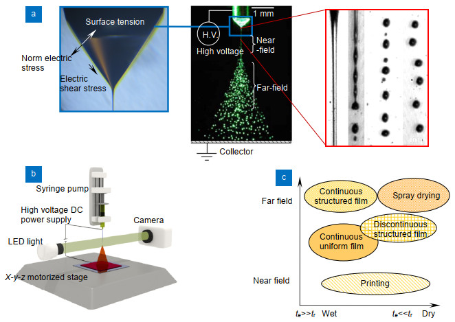
    Fig. 1. The electrospray and electrospray as a tool for material processing.(a) A close-up view of the Taylor cone with a fine jet attached to the cone, and the jet diameter is typically 10 to 104 nm, and details of the break-up process31. (b) A typical arrangement of the electrospray. (c) Several typical outcomes of using electrospray as a material processing tool.
    (a) Electrospray printing setup with three-electrode configuration (emitter, extractor, and ground). (b) Effect of driving field on line width. Inset: electrospray profile images from (left) experiments, (middle) Lagrangian model simulation, and (right) analytical model (Equation (12))21.
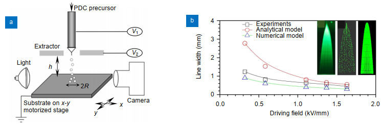
    Fig. 2. (a) Electrospray printing setup with three-electrode configuration (emitter, extractor, and ground). (b) Effect of driving field on line width. Inset: electrospray profile images from (left) experiments, (middle) Lagrangian model simulation, and (right) analytical model (Equation (12))21.
    The impact of a single droplet on the solid and smooth substrate for the inkjet printing17.(a) Side-view of impact process of neutral and charged droplets on mirror-like ITO glass. (b) Neutral droplet and (c) droplet charged at 63 pC. Impacting velocity for both senarios: 0.6 m/s, droplet radius: 1.25 mm48.
    Fig. 3. The impact of a single droplet on the solid and smooth substrate for the inkjet printing17.(a) Side-view of impact process of neutral and charged droplets on mirror-like ITO glass. (b) Neutral droplet and (c) droplet charged at 63 pC. Impacting velocity for both senarios: 0.6 m/s, droplet radius: 1.25 mm48.
    Three typical configurations of multiplexed electrosrpay.(a) Linear array of 19 silica capillaries49. (b) Multi-jet mode with 24 jets stabilized on the grooved nozzle50. (c) The three-electrode design51. (d) Planar array of silicon nozzles51. (e) CNC micromachined linear array made of brass42.
    Fig. 4. Three typical configurations of multiplexed electrosrpay.(a) Linear array of 19 silica capillaries49. (b) Multi-jet mode with 24 jets stabilized on the grooved nozzle50. (c) The three-electrode design51. (d) Planar array of silicon nozzles51. (e) CNC micromachined linear array made of brass42.
    AFM images of the electrosprayed P3HT/PCBM-blend films on the PEDOT/PSS-coated ITO/glass.(a) As-cast. (b) Solvent vapor soaking (SVS). (c) Thermal annealing (TA), and (d) SVS followed by TA. The white line on the AFM images are the cross-section height. The cartoons are schematic illustrations of the P3HT/PCBM morphologies, depicting the nanoscale phase transition of P3HT (wires) and PCBM (balls) as well as the pancake boundary44.
    Fig. 5. AFM images of the electrosprayed P3HT/PCBM-blend films on the PEDOT/PSS-coated ITO/glass.(a) As-cast. (b) Solvent vapor soaking (SVS). (c) Thermal annealing (TA), and (d) SVS followed by TA. The white line on the AFM images are the cross-section height. The cartoons are schematic illustrations of the P3HT/PCBM morphologies, depicting the nanoscale phase transition of P3HT (wires) and PCBM (balls) as well as the pancake boundary44.
    AFM image of the P3HT: PCBM layer. Acetone concentrations45.(a) 5, (b) 10, (c) 15, and (d) 20 vol%. (e) Reference device.
    Fig. 6. AFM image of the P3HT: PCBM layer. Acetone concentrations45.(a) 5, (b) 10, (c) 15, and (d) 20 vol%. (e) Reference device.
    Surface morphology of continuous thin films by electrospray at various flow rates and substrate temperatures (thickness of thin films is ~200 nm)22.(a) Optical microscopy images. (b) AFM images. (c) Raman intensity distribution. (d) Ratio images of Lorentzian components (R) derived from the Raman spectra, Rave: average R value. (e) Current density map by C-AFM and (f) carrier mobility vs. Da numbers.
    Fig. 7. Surface morphology of continuous thin films by electrospray at various flow rates and substrate temperatures (thickness of thin films is ~200 nm)22.(a) Optical microscopy images. (b) AFM images. (c) Raman intensity distribution. (d) Ratio images of Lorentzian components (R) derived from the Raman spectra, Rave: average R value. (e) Current density map by C-AFM and (f) carrier mobility vs. Da numbers.
    SEM images of electrosprayed P3HT films fabricated with different h.(a) Low deposition density at 15.9 mm. (b) 19.6 mm and (c) 23.2 mm. (d) High deposition density at 23.2 mm. (e) GIXRD plot of a spin-cast P3HT film. (f) GIXRD of electrosprayed P3HT film for h= 23.2 mm35.
    Fig. 8. SEM images of electrosprayed P3HT films fabricated with different h.(a) Low deposition density at 15.9 mm. (b) 19.6 mm and (c) 23.2 mm. (d) High deposition density at 23.2 mm. (e) GIXRD plot of a spin-cast P3HT film. (f) GIXRD of electrosprayed P3HT film for h= 23.2 mm35.
    Schematics of (a) electrospray deposition setup, and (b) the formation of perovskite films by electrospray deposition71. The inset photographs show the cone-jet and perovskite film.
    Fig. 9. Schematics of (a) electrospray deposition setup, and (b) the formation of perovskite films by electrospray deposition71. The inset photographs show the cone-jet and perovskite film.
    Top-view SEM images of electrospray printed film when (a)tf>te and (b) when tf te; the scale bar is 1 micron. (c) PCE of electrospray printed and spin-coated devices. Inset: top-view and cross-sectional SEM images of TiO2 films electrospray printed at h=4, 3, 2 mm and spin-coated. Scale bar: 600 nm. (d) PCE of perovskite solar cells by 4 fabrication conditions for Spiro-MeOTAD: electrosprayed with CB or DCB, and spin-coating with CB or DCB. Inset is the corresponding top-view SEM images. Scale bar: 400 nm. (e) Cross-section view SEM image of an all electrospray printed photovoltaic device. (f)J-V curves of the champion cell of the all-printed, all spin-coated devices and the device with only perovskite layer electrospray printed. Inset: PCE histogram of all-electrospray printed devices47.
    Fig. 10. Top-view SEM images of electrospray printed film when (a)tf>te and (b) when tf < te; the scale bar is 1 micron. (c) PCE of electrospray printed and spin-coated devices. Inset: top-view and cross-sectional SEM images of TiO2 films electrospray printed at h=4, 3, 2 mm and spin-coated. Scale bar: 600 nm. (d) PCE of perovskite solar cells by 4 fabrication conditions for Spiro-MeOTAD: electrosprayed with CB or DCB, and spin-coating with CB or DCB. Inset is the corresponding top-view SEM images. Scale bar: 400 nm. (e) Cross-section view SEM image of an all electrospray printed photovoltaic device. (f)J-V curves of the champion cell of the all-printed, all spin-coated devices and the device with only perovskite layer electrospray printed. Inset: PCE histogram of all-electrospray printed devices47.
    Schematic diagram of (a) electrostatic spray and (b) formation of hierarchically structured TiO2 nanospheres100.
    Fig. 11. Schematic diagram of (a) electrostatic spray and (b) formation of hierarchically structured TiO2 nanospheres100.
    SEM images of (a) crack-free photoelectrode of HS TiO2 spheres, (b) cross-sectional image of the HS-TiO2 layer, (c) the non-structured TiO2 layer by electrospray. (d) HS-TiO2 with diameter of 640 nm. (e) HS-TiO2 with diameter of 260 nm. (f) A HS-TiO2 of nanoclusters of P25. (g) After heat treatment at 120 ℃ (for 10 min), and (h) post-treated HS-TiO2 layer with TiCl4 aq. solution100.
    Fig. 12. SEM images of (a) crack-free photoelectrode of HS TiO2 spheres, (b) cross-sectional image of the HS-TiO2 layer, (c) the non-structured TiO2 layer by electrospray. (d) HS-TiO2 with diameter of 640 nm. (e) HS-TiO2 with diameter of 260 nm. (f) A HS-TiO2 of nanoclusters of P25. (g) After heat treatment at 120 ℃ (for 10 min), and (h) post-treated HS-TiO2 layer with TiCl4 aq. solution100.
    SEM image of the ZnO nanoparticles fabricated by (a) doctor-blade method and (b) large scale ZnO film prepared by electrospray technique after heat treated at 460 ℃ for 1 h104.
    Fig. 13. SEM image of the ZnO nanoparticles fabricated by (a) doctor-blade method and (b) large scale ZnO film prepared by electrospray technique after heat treated at 460 ℃ for 1 h104.
    Multiscale of porous structures fabricated by electrospraying dense P25 suspensions. SEM images of the electrosprayed film from dense P25 suspensions to the substrate heated at 150 ℃ and 250 ℃36.(a) Side view of the film showing decent film uniformity. (b) Top view of the electrosprayed film. (c) Closeup of the electrosprayed film showing the multiscale nature of the photo electrode.
    Fig. 14. Multiscale of porous structures fabricated by electrospraying dense P25 suspensions. SEM images of the electrosprayed film from dense P25 suspensions to the substrate heated at 150 ℃ and 250 ℃36.(a) Side view of the film showing decent film uniformity. (b) Top view of the electrosprayed film. (c) Closeup of the electrosprayed film showing the multiscale nature of the photo electrode.
    Comparison of a hybrid electrospray and spin coated DSSC with bilayer structure with a purely spin coated one37.(a) SEM image of hybrid structure with close up of the interface in (b). (c) SEM cross section of a spin coated (5×) DSSC. (d)J–V characteristics comparing the two structures (with the spin coated cell having TiO2 blocking layers and TiCl4 treatment).
    Fig. 15. Comparison of a hybrid electrospray and spin coated DSSC with bilayer structure with a purely spin coated one37.(a) SEM image of hybrid structure with close up of the interface in (b). (c) SEM cross section of a spin coated (5×) DSSC. (d)J–V characteristics comparing the two structures (with the spin coated cell having TiO2 blocking layers and TiCl4 treatment).
    Active layerPerovskitePolymerDSSC
      (DMSO: dimethyl sulfoxide; DMF: N, N-dimethylformamide; DCB: dichlorobenzene; CB: chlorobenzene; OXY: o-xylene; EG: ethylene glycol)
    SolutionNewtonianNon-NewtonianNon-Newtonian (suspension)
    SoluteSaltPolymerTiO2 nanoparticles
    SolventPolar (DMSO, DMF, …)Nonpolar (CB, DCB, OXY, …)Polar (Ethanol, EG, …)
    Electric conductivitiesHigh (~1 S/m)Low (~10-5 S/m)Medium (~10-4 S/m)
    Typical flow rate per source40 μL/h1000 μL/h300 μL/h
    Typical droplet size< 1 μm~20 μm~10 μm
    Typical evaporation time0.1 ms10 ms1 ms
    Table 1. Comparison of electrospray printed active layers of three different solar cells.
    Scalable methodSpecial conditions*Best PCEReferences
      *Special conditions refer to: humidity control, environment control and temperature. The omission of a certain condition means it is not required during the preparation of PSCs.
    Infiltration\12.8%[82]
    Brush printing\9.1%[83]
    Slot-die\12.6%[84]
    Doctor bladeHumidity controlled (15%-25%)10.7%[80]
    Slot-die\12.0%[79]
    Slot-die\14.7%[81]
    Screen-printingHigh-temperature (500 ℃)13.3%[85]
    Blow dryingHigh-temperature (450 ℃), glove box17%[24]
    Electrospray printing\15.0%[47]
    Table 2. Overview of PCE of the reported PSCs with all three layers (ETL, perovskite, and HTL) fabricated using scalable method47.
    Xinyan Zhao, Weiwei Deng. Printing photovoltaics by electrospray[J]. Opto-Electronic Advances, 2020, 3(6): 190038-1
    Download Citation