• Photonics Research
  • Vol. 2, Issue 3, A25 (2014)
Hyunil Byun1, Jinkwon Bok2, Kwansik Cho2, Keunyeong Cho2, Hanmei Choi2, Jinyong Choi2, Sanghun Choi2, Sangdeuk Han2, Seokyong Hong2, Seokhun Hyun2, T. J. Jeong2, Ho-Chul Ji2, In-Sung Joe2, Beomseok Kim2, Donghyun Kim2, Junghye Kim2, Jeong-Kyoum Kim2, Kiho Kim2, Seong-Gu Kim2, Duanhua Kong2, Bongjin Kuh2, Hyuckjoon Kwon2, Beomsuk Lee2, Hocheol Lee2, Kwanghyun Lee2, Shinyoung Lee2, Kyoungwon Na2, Jeongsik Nam2, Amir Nejadmalayeri2, Yongsang Park2, Sunil Parmar2, Junghyung Pyo2, Dongjae Shin2, Joonghan Shin2, Yong-hwack Shin2, Sung-Dong Suh2, Honggoo Yoon2, Yoondong Park2, Junghwan Choi2, Kyoung-Ho Ha2, and and Gitae Jeong2
Author Affiliations
  • 1Samsung Electronics, 1 Samsungjeonjaro, Hwasungshi, Gyoung-gido, 445-330, South Korea
  • 2the same as above
  • show less
    DOI: 10.1364/PRJ.2.000A25 Cite this Article Set citation alerts
    Hyunil Byun, Jinkwon Bok, Kwansik Cho, Keunyeong Cho, Hanmei Choi, Jinyong Choi, Sanghun Choi, Sangdeuk Han, Seokyong Hong, Seokhun Hyun, T. J. Jeong, Ho-Chul Ji, In-Sung Joe, Beomseok Kim, Donghyun Kim, Junghye Kim, Jeong-Kyoum Kim, Kiho Kim, Seong-Gu Kim, Duanhua Kong, Bongjin Kuh, Hyuckjoon Kwon, Beomsuk Lee, Hocheol Lee, Kwanghyun Lee, Shinyoung Lee, Kyoungwon Na, Jeongsik Nam, Amir Nejadmalayeri, Yongsang Park, Sunil Parmar, Junghyung Pyo, Dongjae Shin, Joonghan Shin, Yong-hwack Shin, Sung-Dong Suh, Honggoo Yoon, Yoondong Park, Junghwan Choi, Kyoung-Ho Ha, and Gitae Jeong. Bulk-Si photonics technology for DRAM interface [Invited][J]. Photonics Research, 2014, 2(3): A25 Copy Citation Text show less
    Simulated eye diagrams of memory bus with 4 DIMMs in one DDR3 memory channel.
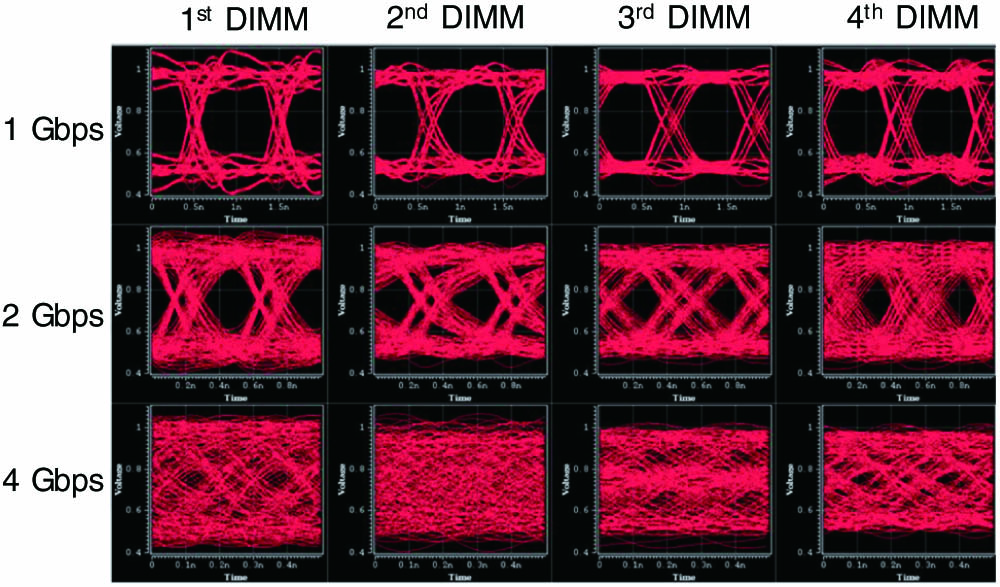
    Fig. 1. Simulated eye diagrams of memory bus with 4 DIMMs in one DDR3 memory channel.
    Process steps for fabricating the waveguide on a bulk-Si substrate. C-Si: crystallized silicon, PR: photoresist.
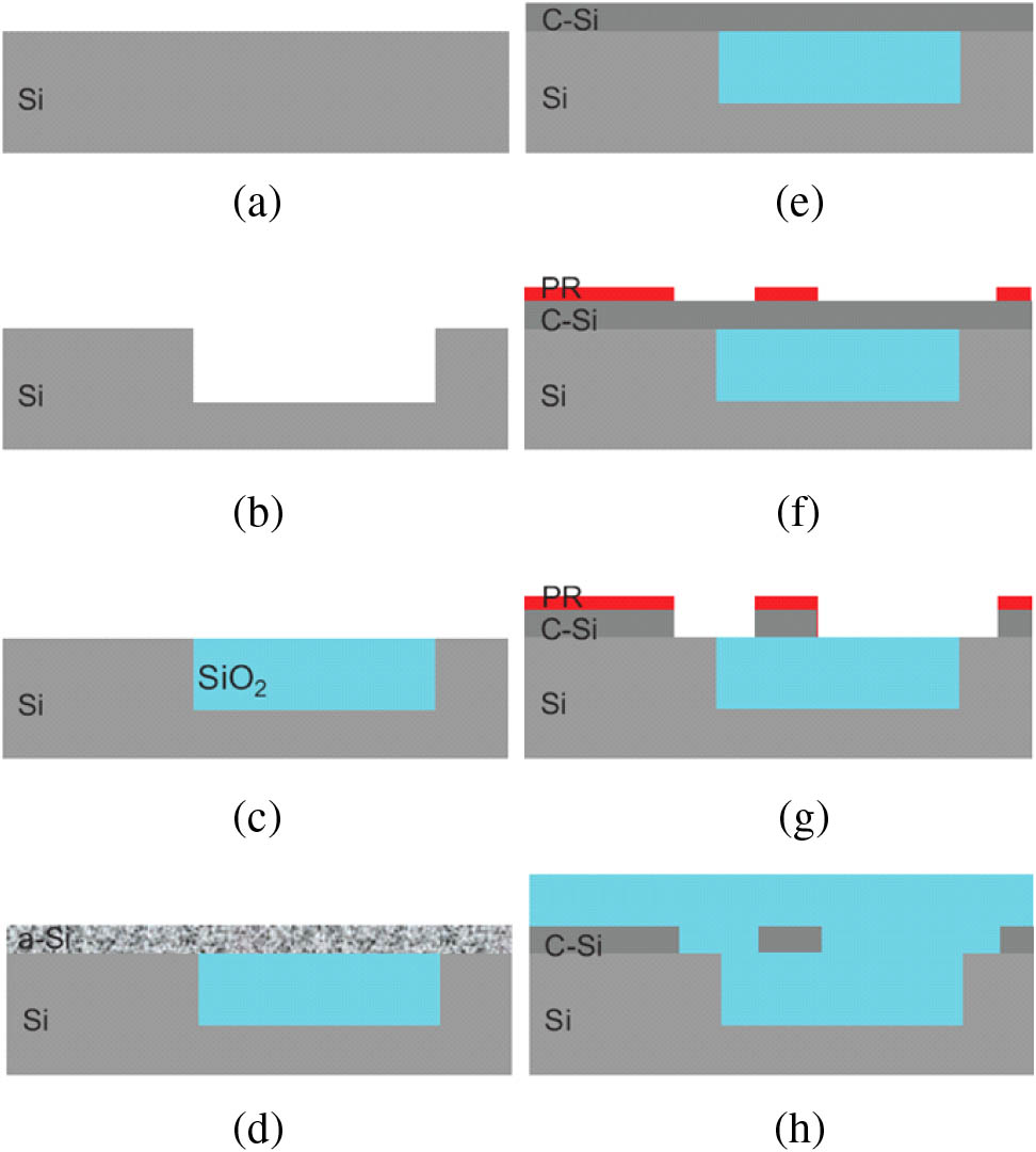
    Fig. 2. Process steps for fabricating the waveguide on a bulk-Si substrate. C-Si: crystallized silicon, PR: photoresist.
    SEM images after crystallization of deposited a-Si depending on annealing condition: (a) low, (b) medium, and (c) high temperature.
    Fig. 3. SEM images after crystallization of deposited a-Si depending on annealing condition: (a) low, (b) medium, and (c) high temperature.
    VSEM images of fabricated waveguide on the bulk-Si substrate.
    Fig. 4. VSEM images of fabricated waveguide on the bulk-Si substrate.
    Cross section of inlaid structure for LEG process.
    Fig. 5. Cross section of inlaid structure for LEG process.
    High resolution TEM image and diffraction pattern: (a) SPE-Si and (b) LEG-Si.
    Fig. 6. High resolution TEM image and diffraction pattern: (a) SPE-Si and (b) LEG-Si.
    (a) Cross-sectional diagram of the active part of the bulk-Si MZI modulator. (b) SEM image of the dotted region in (a). The inclined arrows indicate the boundary of the local oxide undercladding formed underneath the active part. (c) Microscope image. Dotted line indicates the location of (a) and (b).
    Fig. 7. (a) Cross-sectional diagram of the active part of the bulk-Si MZI modulator. (b) SEM image of the dotted region in (a). The inclined arrows indicate the boundary of the local oxide undercladding formed underneath the active part. (c) Microscope image. Dotted line indicates the location of (a) and (b).
    Optical eye diagrams at NRZ 231–1 PRBS signal at (a) 5 Gb/s without de-emphasis and (b) 10 Gb/s with de-emphasis.
    Fig. 8. Optical eye diagrams at NRZ 2311 PRBS signal at (a) 5Gb/s without de-emphasis and (b) 10Gb/s with de-emphasis.
    (a) Lateral design of racetrack modulator with metal boundary illustrated. (b) Eye diagram at 1559.24 nm with 2.5 Vpp driving.
    Fig. 9. (a) Lateral design of racetrack modulator with metal boundary illustrated. (b) Eye diagram at 1559.24 nm with 2.5Vpp driving.
    (a) Microscope photography, (b) SEM image, and (c) 25 Gbp/s eye diagram of Ge/Si surface photodetector.
    Fig. 10. (a) Microscope photography, (b) SEM image, and (c) 25Gbp/s eye diagram of Ge/Si surface photodetector.
    Schematic diagram of waveguide-type photodetector (a) along the light propagation, and (b) perpendicular to the light propagation. (c) VSEM image, (d) 15 Gb/s eye diagram at −1 V bias, and (e) 25 Gb/s eye diagram at −7 V bias.
    Fig. 11. Schematic diagram of waveguide-type photodetector (a) along the light propagation, and (b) perpendicular to the light propagation. (c) VSEM image, (d) 15Gb/s eye diagram at 1V bias, and (e) 25Gb/s eye diagram at 7V bias.
    (a) Optical microscope image of EPIC, (b) schematic of EPIC vertical structure, and (c) SEM images of transistors, modulator, and Ge photodiode.
    Fig. 12. (a) Optical microscope image of EPIC, (b) schematic of EPIC vertical structure, and (c) SEM images of transistors, modulator, and Ge photodiode.
    Performance of the bulk-Si photonic devices integrated into the DRAM process.
    Fig. 13. Performance of the bulk-Si photonic devices integrated into the DRAM process.
    1×4 optical link configuration for multidrop memory bus.
    Fig. 14. 1×4 optical link configuration for multidrop memory bus.
    Electrical eye diagram measured at channel 1–4 receiver: (a) through (d) with the transmitter in a QFP package, (e) through (h) on a bare die.
    Fig. 15. Electrical eye diagram measured at channel 1–4 receiver: (a) through (d) with the transmitter in a QFP package, (e) through (h) on a bare die.
    Block diagram of an optical interconnect transceiver. PD: photodiode, MOD: modulator.
    Fig. 16. Block diagram of an optical interconnect transceiver. PD: photodiode, MOD: modulator.
    (a) Photograph of dies for PIC and EIC. (b) Photograph of copackaged optical transceiver chip.
    Fig. 17. (a) Photograph of dies for PIC and EIC. (b) Photograph of copackaged optical transceiver chip.
    (a) Experiment setup to verify link operation using two optical transceivers. (b) and (c) Eye diagram at the output of optical amplifier at data rate of 1.5 and 2.5 Gb/s.
    Fig. 18. (a) Experiment setup to verify link operation using two optical transceivers. (b) and (c) Eye diagram at the output of optical amplifier at data rate of 1.5 and 2.5Gb/s.
    (a) Photograph and (b) block diagram of the experiment setup to verify optically interconnected DRAM interface. A: optical amplifier.
    Fig. 19. (a) Photograph and (b) block diagram of the experiment setup to verify optically interconnected DRAM interface. A: optical amplifier.
    (a) Block diagram of the experiment setup and (b) oscilloscope traces for DQ0 (blue) and DQS signals (red) at controller side and DRAM side with output enable signals (green).
    Fig. 20. (a) Block diagram of the experiment setup and (b) oscilloscope traces for DQ0 (blue) and DQS signals (red) at controller side and DRAM side with output enable signals (green).
    Hyunil Byun, Jinkwon Bok, Kwansik Cho, Keunyeong Cho, Hanmei Choi, Jinyong Choi, Sanghun Choi, Sangdeuk Han, Seokyong Hong, Seokhun Hyun, T. J. Jeong, Ho-Chul Ji, In-Sung Joe, Beomseok Kim, Donghyun Kim, Junghye Kim, Jeong-Kyoum Kim, Kiho Kim, Seong-Gu Kim, Duanhua Kong, Bongjin Kuh, Hyuckjoon Kwon, Beomsuk Lee, Hocheol Lee, Kwanghyun Lee, Shinyoung Lee, Kyoungwon Na, Jeongsik Nam, Amir Nejadmalayeri, Yongsang Park, Sunil Parmar, Junghyung Pyo, Dongjae Shin, Joonghan Shin, Yong-hwack Shin, Sung-Dong Suh, Honggoo Yoon, Yoondong Park, Junghwan Choi, Kyoung-Ho Ha, and Gitae Jeong. Bulk-Si photonics technology for DRAM interface [Invited][J]. Photonics Research, 2014, 2(3): A25
    Download Citation