• Opto-Electronic Advances
  • Vol. 2, Issue 2, 180025 (2019)
Lei Li1, Liang Xiao1, Jinhui Wang1, and Qionghua Wang2、*
Author Affiliations
  • 1School of Electronics and Information Engineering, Sichuan University, Chengdu 610065, China
  • 2School of Instrumentation Science and Opto-electronics Engineering, Beihang University, Beijing 100191, China
  • show less
    DOI: 10.29026/oea.2019.180025 Cite this Article
    Lei Li, Liang Xiao, Jinhui Wang, Qionghua Wang. Movable electrowetting optofluidic lens for optical axial scanning in microscopy[J]. Opto-Electronic Advances, 2019, 2(2): 180025 Copy Citation Text show less
    Schematic cross-sectional structure and operating mechanism of the movable electrowetting optofluidic lens.(a) Cell structure. The curvature of the silicone oil (yellow)-conductive liquid (blue) interface in the central aperture is regulated by the external voltages. (b) Moving actuation. When the external voltages U1 and U3 are applied, the L-L interface moves downwards. (c) Deforming actuation. When external voltage U2 and U4 are applied, the L-L interface deforms. (d) Working principle of axial scanning.
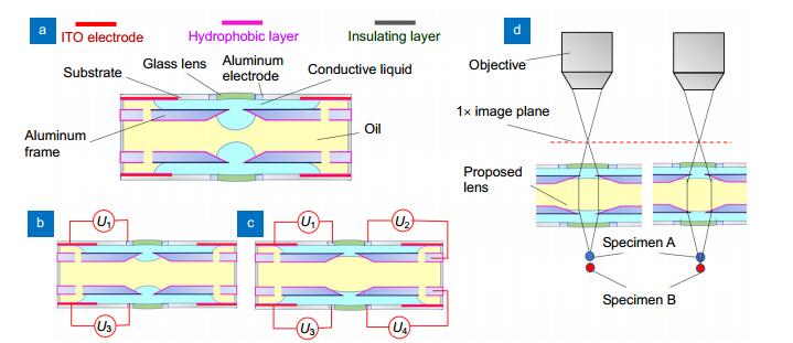
    Fig. 1. Schematic cross-sectional structure and operating mechanism of the movable electrowetting optofluidic lens.(a) Cell structure. The curvature of the silicone oil (yellow)-conductive liquid (blue) interface in the central aperture is regulated by the external voltages. (b) Moving actuation. When the external voltages U1 and U3 are applied, the L-L interface moves downwards. (c) Deforming actuation. When external voltage U2 and U4 are applied, the L-L interface deforms. (d) Working principle of axial scanning.
    Performance of moving and deforming actuation of the movable electrowetting optofluidic lens.(a) Cell structure. (b) State 1, UA= 0 V, UB=0 V. (c) State 2, UA=50 V, UB=0 V. (d) State 3, UA=50 V, UB=60 V, t=0 s. (e) State 3, UA=50 V, UB=60 V, t=1 s. (f) Shift distance with different voltages.
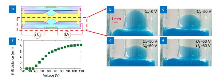
    Fig. 2. Performance of moving and deforming actuation of the movable electrowetting optofluidic lens.(a) Cell structure. (b) State 1, UA= 0 V, UB=0 V. (c) State 2, UA=50 V, UB=0 V. (d) State 3, UA=50 V, UB=60 V, t=0 s. (e) State 3, UA=50 V, UB=60 V, t=1 s. (f) Shift distance with different voltages.
    Fabricated prototype of the movable electrowetting optofluidic lens.(a) All the elements of the device. (b) Assembled prototype (Side view). (c) Assembled prototype (Top view).
    Fig. 3. Fabricated prototype of the movable electrowetting optofluidic lens.(a) All the elements of the device. (b) Assembled prototype (Side view). (c) Assembled prototype (Top view).
    (a) Simulation of the movable electrowetting optofluidic lens. (b) MTF for 20 mm object distance. (c) MTF for 20.5 mm object distance. (d) MTF for 21 mm object distance.
    Fig. 4. (a) Simulation of the movable electrowetting optofluidic lens. (b) MTF for 20 mm object distance. (c) MTF for 20.5 mm object distance. (d) MTF for 21 mm object distance.
    Imaging experiment using the movable electrowetting optofluidic lens.(a) Experiment setup. (b) Specimen A. (c) Specimen B. (d) Specimen A and B stacked together. (e) Focusing on specimen A. (f) Focusing on specimen B.
    Fig. 5. Imaging experiment using the movable electrowetting optofluidic lens.(a) Experiment setup. (b) Specimen A. (c) Specimen B. (d) Specimen A and B stacked together. (e) Focusing on specimen A. (f) Focusing on specimen B.
    Objective distanceBack focal lengthShift distance of the L-L interfaceMagnification
    20 mm20 mm0 mm
    20.5 mm20 mm0.5 mm
    21 mm20 mm1 mm
    Table 1. Parameter of the device in simulation for axial scanning
    Lei Li, Liang Xiao, Jinhui Wang, Qionghua Wang. Movable electrowetting optofluidic lens for optical axial scanning in microscopy[J]. Opto-Electronic Advances, 2019, 2(2): 180025
    Download Citation