• Laser & Optoelectronics Progress
  • Vol. 59, Issue 4, 0405001 (2022)
Feng Gao, Chenyue Zhu, Jingyue Li, Chunyan Wu*, and Linbao Luo
Author Affiliations
  • School of Electronic Science and Applied Physics, Hefei University of Technology, Hefei , Anhui 230601, China
  • show less
    DOI: 10.3788/LOP202259.0405001 Cite this Article Set citation alerts
    Feng Gao, Chenyue Zhu, Jingyue Li, Chunyan Wu, Linbao Luo. ITO-Based Active Metasurfaces with Phase Tunability[J]. Laser & Optoelectronics Progress, 2022, 59(4): 0405001 Copy Citation Text show less
    Electrical simulation results. (a) Schematic of electrically tunable ITO metasurface, the MOS structure consists of a gold back plane, a thin ITO film, a thin Al2O3 film, and gold stripe nanoantenna array; (b) spatial distribution of the carrier concentration under different applied voltages; (c)(d) distribution diagrams of the permittivity of ITO at different voltages and depths at a wavelength of 1470 nm
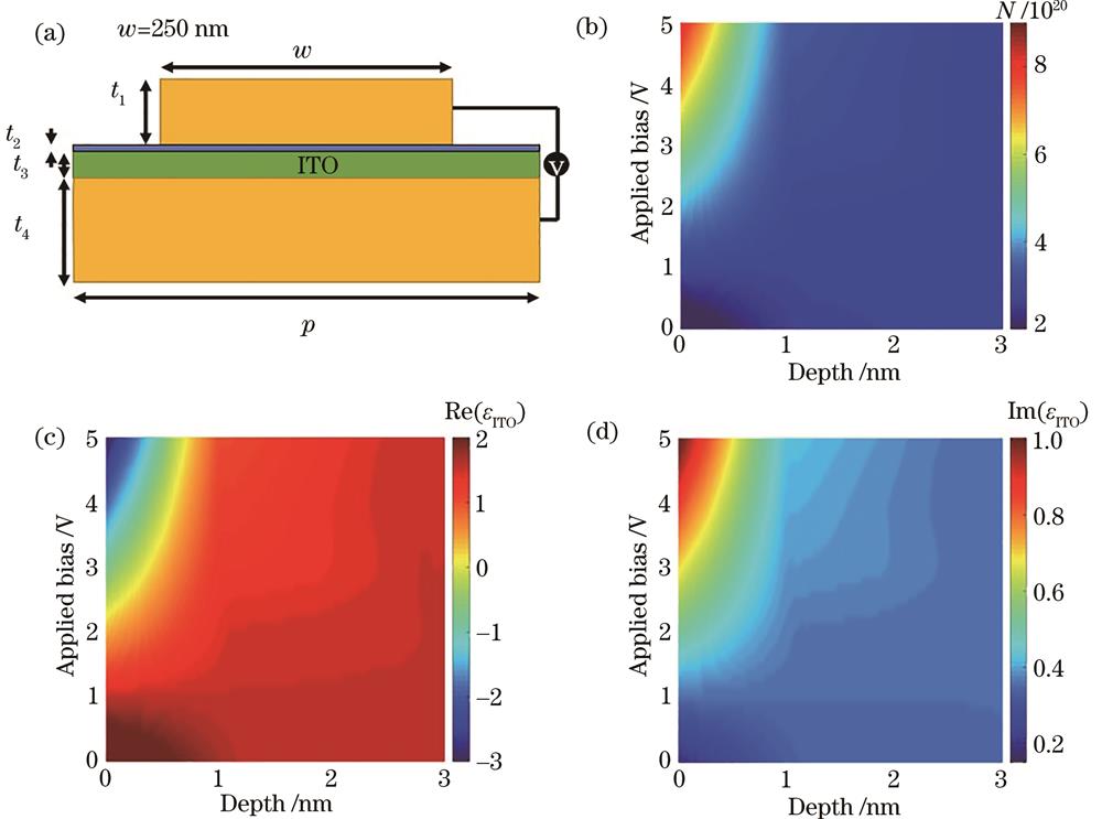
    Fig. 1. Electrical simulation results. (a) Schematic of electrically tunable ITO metasurface, the MOS structure consists of a gold back plane, a thin ITO film, a thin Al2O3 film, and gold stripe nanoantenna array; (b) spatial distribution of the carrier concentration under different applied voltages; (c)(d) distribution diagrams of the permittivity of ITO at different voltages and depths at a wavelength of 1470 nm
    MOS structure with charge accumulation (dash) and charge depletion (solid). (a) Schematic of MOS structure; (b) energy-band diagram; (c) carrier density curve; (d) as the carrier density increases or decreases at the interface, the real part of the permittivity changes from positive to negative
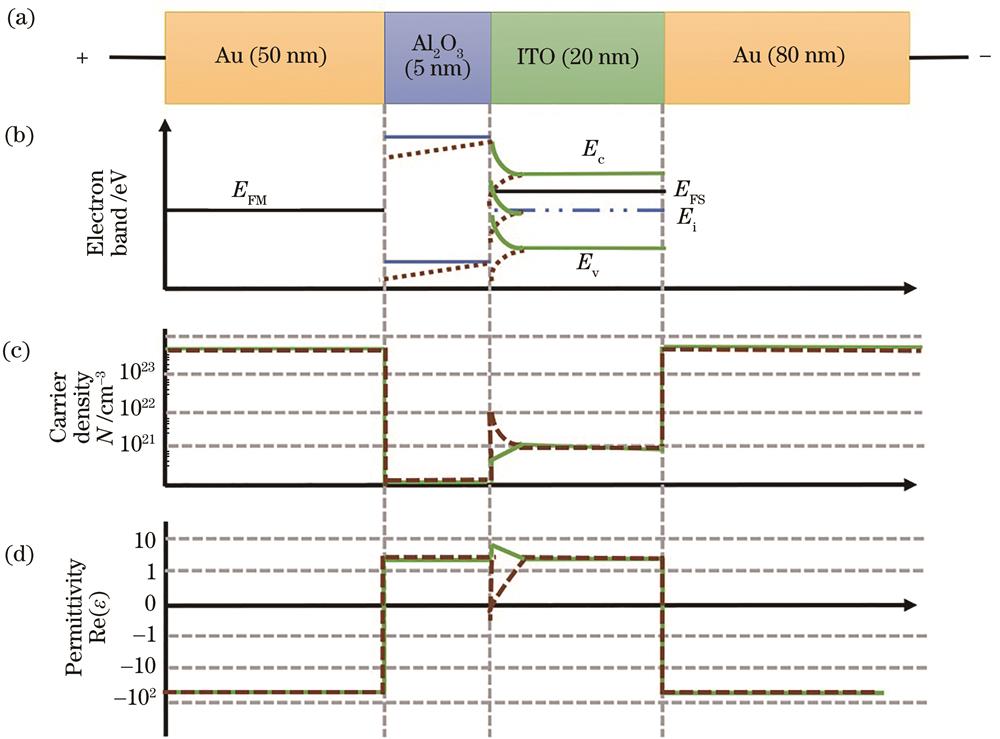
    Fig. 2. MOS structure with charge accumulation (dash) and charge depletion (solid). (a) Schematic of MOS structure; (b) energy-band diagram; (c) carrier density curve; (d) as the carrier density increases or decreases at the interface, the real part of the permittivity changes from positive to negative
    Optical simulation results of adjustable metasurface. (a) Reflection phase as a function of voltage and wavelength; (b) reflectance as a function of voltage and wavelength; (c)‒(e) spatial distribution of the electric field Ey at 1470-nm wavelength under applied bias of 0, 2.5, 5 V, respectively
    Fig. 3. Optical simulation results of adjustable metasurface. (a) Reflection phase as a function of voltage and wavelength; (b) reflectance as a function of voltage and wavelength; (c)‒(e) spatial distribution of the electric field Ey at 1470-nm wavelength under applied bias of 0, 2.5, 5 V, respectively
    Practical applications of deflection and focusing. (a) Schematic of the electrically tunable reflectarray antenna; (b) simulated electric field distribution with the bending angle of -18o; (c) simulated relationship between the reflection amplitude and the angle; (d) electric field distribution at focal length of 6λ
    Fig. 4. Practical applications of deflection and focusing. (a) Schematic of the electrically tunable reflectarray antenna; (b) simulated electric field distribution with the bending angle of -18o; (c) simulated relationship between the reflection amplitude and the angle; (d) electric field distribution at focal length of 6λ
    Double-gated metasurface. (a) Schematic of the unit cell of the double-gated metasurface, the thicknesses of the antenna array, the gate dielectrics, the ITO layer, and the back reflector are t1= 50 nm, t2=9.5 nm, t3=5 nm, and t4= 80 nm, respectively, and the electrode width is w2=170 nm; (b) simulated result of charge carrier distribution; (c) real part of the dielectric permittivity of the ITO as a function of the applied voltage and position; (d) maximum phase achieved under different voltages at λ=1500 nm
    Fig. 5. Double-gated metasurface. (a) Schematic of the unit cell of the double-gated metasurface, the thicknesses of the antenna array, the gate dielectrics, the ITO layer, and the back reflector are t1= 50 nm, t2=9.5 nm, t3=5 nm, and t4= 80 nm, respectively, and the electrode width is w2=170 nm; (b) simulated result of charge carrier distribution; (c) real part of the dielectric permittivity of the ITO as a function of the applied voltage and position; (d) maximum phase achieved under different voltages at λ=1500 nm
    Number12345678910
    Phase /(o-52-236356493122151180209
    Voltage /V00.81.351.762.122.462.823.213.724.55
    Table 1. Phase and voltage values of each antenna in deflection applications
    Feng Gao, Chenyue Zhu, Jingyue Li, Chunyan Wu, Linbao Luo. ITO-Based Active Metasurfaces with Phase Tunability[J]. Laser & Optoelectronics Progress, 2022, 59(4): 0405001
    Download Citation