
Zhou Wang, Xinyi Shan, Xugao Cui, Pengfei Tian. Characteristics and techniques of GaN-based micro-LEDs for application in next-generation display[J]. Journal of Semiconductors, 2020, 41(4): 041606
- Journal of Semiconductors
- Vol. 41, Issue 4, 041606 (2020)
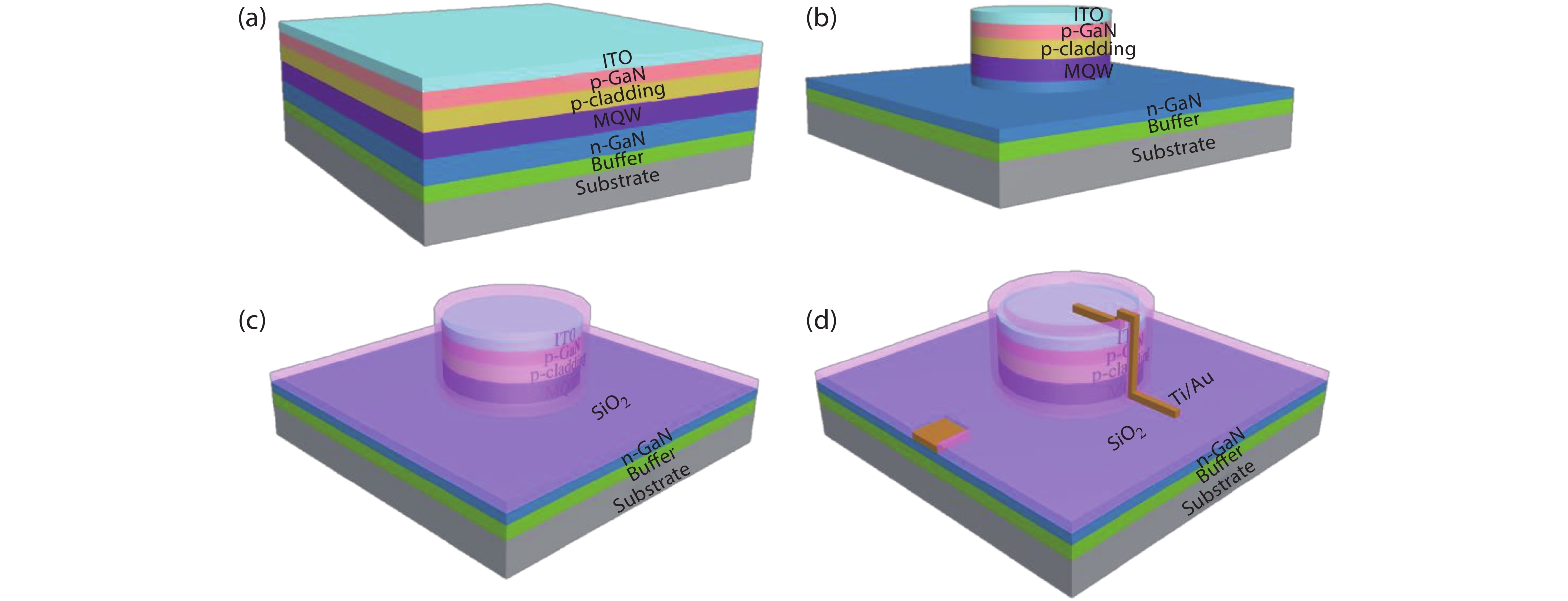
Fig. 1. (Color online) (a) The GaN-based epitaxial structure with silicon substrate. (b) Etching to n-GaN layer to form a micro-LED mesa array. (c) The deposition of SiO2 through PECVD. (d) The deposition of Ti/Au to serve as electrodes.
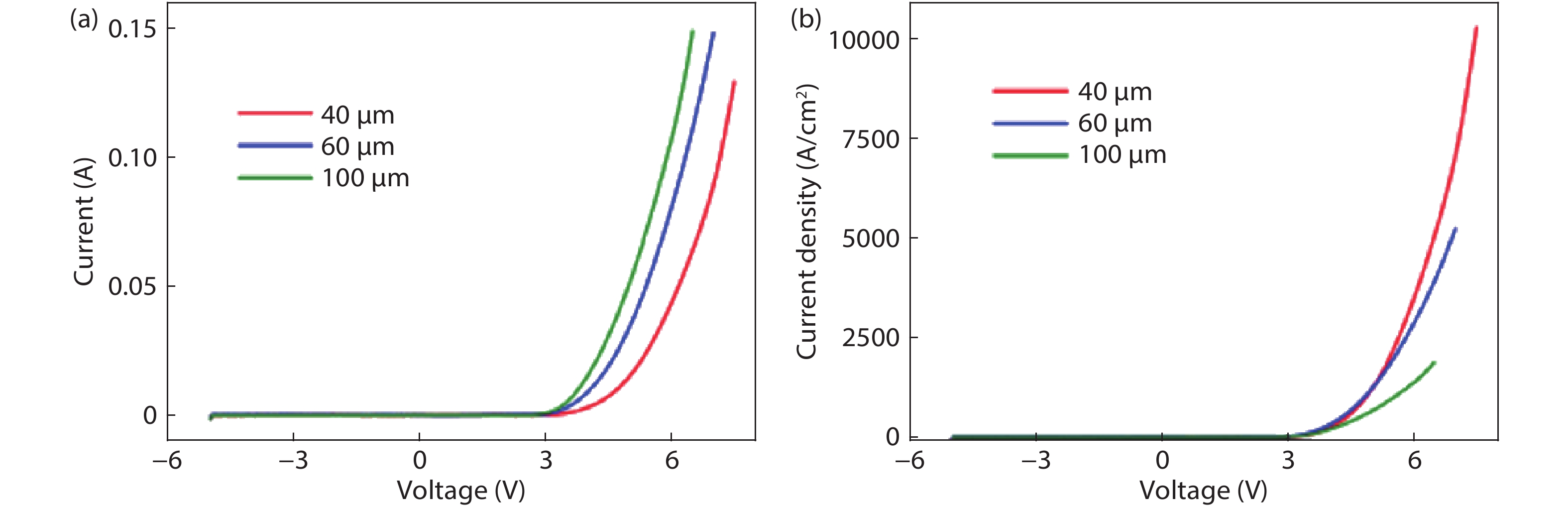
Fig. 2. (Color online) (a) I–V curves of blue micro-LED pixels with different sizes. (b) The curve of current density for blue micro-LED with different sizes.
Fig. 3. (Color online) (a) L–I curves of blue micro-LEDs with different diameters. (b) The curve of the light-output power density versus injection current density for blue micro-LED with different sizes.
Fig. 4. (Color online) (a) EQE versus current density from 300 to 500 K with 25 K temperature increment on a semi-logarithmic scale. (b) Bandwidth versus current from 300 to 425 K to show the trend with temperature[25 ]. Copyright 2014, Applied Physics Letters.
Fig. 5. (Color online) (a) The schematic of passive matrix micro-LED array[16 ]. (b) The schematic of active matrix micro-LED array[28 ]. Copyright 2015, IEEE Transactions on Electron Devices.
Fig. 6. (Color online) Schematic of transfer printing using capillary bonding. (a) Using an elastomeric stamp for the pick-up of a suspended micro-LED. (b) Upon pick-up, micro-LED is compressed against an acetone-wetted cloth. (c) Released micro-LED when the backside contacts receiving substrate. (d) After thermal curing, the micro-LED is bonded to the new substrate[19 ]. Copyright 2015, Optics Express.
Fig. 7. (Color online) (a) Standard MQW LED was grown on sapphire substrates for the micro-LED arrays. (b) The using of aerosol jet printing method to spray the red QDs on the micro-LED array. (c) The spraying of green QDs on the micro-LED array. (d) The spraying of blue QDs on the micro-LED array. (e) The DBR was added to the top of micro LED arrays[20 ]. Copyright 2015, Optic Express.
Fig. 8. (Color online) Schematic of the fabrication process for the RGB LED pixel. (a) The fabrication of nanopillar structures by photolithography and etching. (b) Planarization and electrical insulation treatment. (c) Formation of electrical interconnect[21 ]. Copyright 2017, Applied Physics Letters.
|
Table 1. The comparison of main characteristics of micro-LED, LCD, and OLED.

Set citation alerts for the article
Please enter your email address
© Copyright 2018-2021 | Chinese Laser Press. All Rights Reserved 沪ICP备15018463号-20