
Zhou Wang, Xinyi Shan, Xugao Cui, Pengfei Tian. Characteristics and techniques of GaN-based micro-LEDs for application in next-generation display[J]. Journal of Semiconductors, 2020, 41(4): 041606
- Journal of Semiconductors
- Vol. 41, Issue 4, 041606 (2020)
Abstract
1. Introduction
From plasma display panel (PDP), cathode ray tube (CRT) to liquid crystal display (LCD), and then to organic light-emitting diode (OLED) and quantum dot light-emitting diode (QLED), the competition for the new generation of display technology has never stopped the pace. As the OLED and QLED challenge the LCD and dominate the whole display market, micro-LED has entered the field of vision because of its excellent properties of high brightness, great color gamut, fast response time, outstanding power efficiency, high stability and so on[
As shown in Table 1, micro-LED has advantages of excellent image quality, superior stability and other outstanding factors compared with LCD and OLED[
Sony, Apple, Samsung and many academic researchers regard micro-LED as the next-generation display, and continue to increase the research investment. However, there still exist several challenges of micro-LED display technology, such as massive transfer and full-color display of micro-LEDs. At present, the full-color display of micro-LED can be achieved by transfer printing red, green and blue (RGB) micro-LED, exciting quantum dots (QDs) to achieve full color, and designing RGB micro-LED pixels on the same wafer through local strain engineering and growth[
2. The basic micro-LED processing techniques
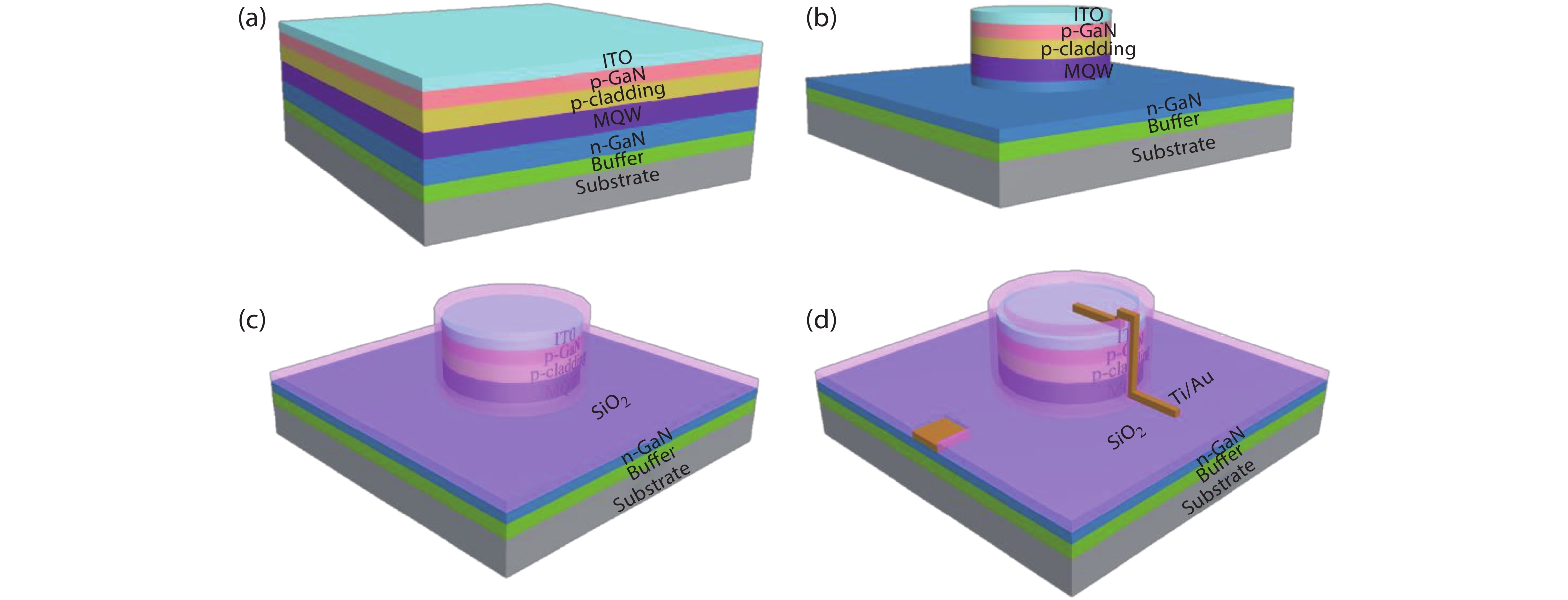
For micro-LED processing, the metal-organic chemical vapor deposition (MOCVD) is used to perform the epitaxial layer growth on the substrate. For example, the epitaxial GaN wafers grown on silicon substrate are introduced, and then chip fabrication process is carried out. The reason of making use of silicon as substrate here is that it has the advantages of large size, low cost, high thermal conductivity and can be integrated with Si based microelectronic devices. Also the silicon substrate has more advantages in the growth of high-efficiency LED with long emission wavelength, such as red, green and yellow[
![]()
Figure 1.(Color online) (a) The GaN-based epitaxial structure with silicon substrate. (b) Etching to n-GaN layer to form a micro-LED mesa array. (c) The deposition of SiO2 through PECVD. (d) The deposition of Ti/Au to serve as electrodes.
3. The performances of micro-LED
Herein, many performance tests have been carried out to verify the excellent characteristics of micro-LED. The I–V characteristics of micro-LED are similar to those of p–n junction diode in classical semiconductor theory. From the I–V curves of blue micro-LED pixels with different diameters prepared on the same epitaxial wafer, series resistance of the pixels increase with the decrease of chip size, as shown in Fig. 2(a)[
![]()
Figure 2.(Color online) (a)
Optical properties are one of the fundamental and important properties of micro-LEDs, so other tests such as L–I also have been carried out. As shown in Fig. 3(a), it can be seen from the curve that the maximum output power increases with the increase of pixel size at the same current. And the curve of the corresponding light-output power versus current density is shown in Fig. 3(b). The smaller size of micro-LED devices, the higher maximum optical power density that can be output, and the smaller micro-LED devices can sustain higher injection current density according to the Fig. 2. The results also indicate that micro-LED has the advantages of high saturation current density and high light-output power density. Based on these performance tests, the brightness of micro-LED display can be up to 100 000 cd/m2[
![]()
Figure 3.(Color online) (a)
After the corresponding electrical and optical properties were tested, the external quantum efficiency (EQE) and bandwidth were also analyzed[
![]()
Figure 4.(Color online) (a) EQE versus current density from 300 to 500 K with 25 K temperature increment on a semi-logarithmic scale. (b) Bandwidth versus current from 300 to 425 K to show the trend with temperature[
4. The key micro-LED technology in full color display
The driving modes of micro-LED are divided into passive matrix and active matrix[
![]()
Figure 5.(Color online) (a) The schematic of passive matrix micro-LED array[
Also for the full-color display scheme, because of the continuous research of colorization and high brightness, many full-color display techniques have been developed, including RGB tricolor LED method by transfer printing red, green and blue micro-LEDs, UV or blue LED exciting color converters, and RGB micro-LED pixel through local strain engineering.
As shown in Fig. 6, the transfer printing scheme will be introduced. Capillary bonding is achieved by introducing an intermediate step to the transfer printing process, in which the substrate of the micro-LED being transferred is underetched by KOH solution[
![]()
Figure 6.(Color online) Schematic of transfer printing using capillary bonding. (a) Using an elastomeric stamp for the pick-up of a suspended micro-LED. (b) Upon pick-up, micro-LED is compressed against an acetone-wetted cloth. (c) Released micro-LED when the backside contacts receiving substrate. (d) After thermal curing, the micro-LED is bonded to the new substrate[
At present, the massive transfer of micro-LED is still a bottleneck. The main technical challenges include the requirement of very high stability and accuracy of the transfer process. For RGB full-color display, as only single-color high-efficiency micro-LED can be developed on the same substrate, it is necessary to transfer the RGB micro-LEDs separately from different substrates, which requires very accurate technology to transfer a large amount of micro-LEDs that results in increasing difficulty of the transfer process.
Due to the high efficiency characteristics, the RGB technique may be the mainstream technique in the future[
Here color conversion technique has also been researched, which mainly uses UV micro-LED to stimulate red, green and blue luminescent medium such as phosphor or QDs to produce light of specific wavelength, and then full-color display can be achieved through matching the tricolor[
![]()
Figure 7.(Color online) (a) Standard MQW LED was grown on sapphire substrates for the micro-LED arrays. (b) The using of aerosol jet printing method to spray the red QDs on the micro-LED array. (c) The spraying of green QDs on the micro-LED array. (d) The spraying of blue QDs on the micro-LED array. (e) The DBR was added to the top of micro LED arrays[
Growth methods, such as strain engineering method after the growth of epitaxial layer and chip fabrication, also have been designed to achieve full color on the same wafer[
![]()
Figure 8.(Color online) Schematic of the fabrication process for the RGB LED pixel. (a) The fabrication of nanopillar structures by photolithography and etching. (b) Planarization and electrical insulation treatment. (c) Formation of electrical interconnect[
There are also many other full-color display schemes, such as optical lens synthesis. The RGB micro-LED arrays were packaged on three packaging boards respectively and connected with a control board and a trichromatic prism, and then the brightness of the trichromatic micro-LED is adjusted to achieve colorization[
5. Conclusion
This review paper has described the basic characteristics and techniques of micro-LED for next-generation full-color display, mainly including the preparation process, the characteristics compared with LCD and OLED display, the related electrical performance and optical performance, and the full color techniques. With the development of micro-LED, it is expected that micro-LED will play an important role in academia and industry in the future display.
Acknowledgements
This work was supported by National Natural Science Foundation of China (NSFC) (61974031, 61705041 and 61571135); Shanghai Sailing Program (17YF1429100); Shanghai Technical Standard Program (18DZ2206000); State Key Laboratory of Intense Pulsed Radiation Simulation and Effect Funding (SKLIPR1607); National Key Research and Development Program of China (2017YFB0403603).
References
[1] H E Lee, J H Shin, J H Park et al. Micro light-emitting diodes for display and flexible biomedical applications. Adv Funct Mater, 29, 1808075(2019).
[2] H E Lee, J Choi, S H Lee et al. Monolithic flexible vertical GaN light-emitting diodes for a transparent wireless brain optical stimulator. Adv Mater, 30, 1800649(2018).
[3] P Yang, L Zhang, D J Kang et al. High-resolution inkjet printing of quantum dot light-emitting microdiode arrays. Adv Opt Mater, 8, 1901429(2019).
[4] W Yang, S Zhang, J J D McKendry et al. Size-dependent capacitance study on InGaN-based micro-light-emitting diodes. J Appl Phys, 116, 044512(2014).
[5] P Tian, J J D McKendry, Z Gong et al. Characteristics and applications of micro-pixelated GaN-based light emitting diodes on Si substrates. J Appl Phys, 115, 033112(2014).
[6] Y Li, Q Wu, F Y Meng et al. Enhanced performance of large-area vertical light-emitting diodes treated by laser irradiation. Micro Nano Lett, 12, 369(2017).
[7] X Chen, F Kong, K Li et al. Study of light extraction efficiency of flip-chip GaN-based LEDs with different periodic arrays. Opt Commun, 314, 90(2014).
[8] Y C Yao, J M Hwang, Z P Yang et al. Enhanced external quantum efficiency in GaN-based vertical-type light-emitting diodes by localized surface plasmons. Sci Rep, 6, 22659(2016).
[9] Z Liu, W C Chong, K M Wong et al. GaN-based LED micro-displays for wearable applications. Microelectron Eng, 148, 98(2015).
[10] C C Lin, Y H Fang, M J Kao et al. Ultra-fine pitch thin-film micro LED display for indoor applications. SID Symp Dig Tech Pap, 49, 782(2018).
[11] J K Yoon, E M Park, J S Son et al. The study of picture quality of OLED TV with WRGB OLEDs structure. SID Symp Dig Tech Pap, 44, 326(2013).
[12] S Katsui, H Kobayashi, T Nakagawa et al. 5291-PPI organic light-emitting diode display using field-effect transistors including a c-axis aligned crystalline oxide semiconductor. SID Symp Dig Tech Pap, 50, 311(2019).
[13]
[14]
[15] J M M Santos, B E Jones, P J Schlosser et al. Hybrid GaN LED with capillary-bonded II–VI MQW color-converting membrane for visible light communications. Semicond Sci Tech, 30, 035012(2015).
[16] A Hori, D Yasunaga, A Satake et al. Temperature and injection current dependence of electroluminescence intensity in green and blue InGaN single-quantum-well light-emitting diodes. J Appl Phys, 93, 3152(2003).
[17]
[18] M Q Fei, Y Fei. The wide view-angle technique of TFT-LCD. Adv Display, 11, 22(2008).
[19] A J Trindade, B Guilhabert, E Y Xie et al. Heterogeneous integration of gallium nitride light-emitting diodes on diamond and silica by transfer printing. Opt Express, 23, 9329(2015).
[20] H V Han, H Y Lin, C C Lin et al. Resonant-enhanced full-color emission of quantum-dot-based micro LED display technology. Opt Express, 23, 32504(2015).
[21] K Chung, J Sui, B Demory et al. Color mixing from monolithically integrated InGaN-based light-emitting diodes by local strain engineering. Appl Phys Lett, 111, 041101(2017).
[22] F Jiang, J Zhang, L Xu et al. Efficient InGaN-based yellow-light-emitting diodes. Photonics Res, 7, 144(2019).
[23] P Tian, J J McKendry, E Gu et al. Fabrication, characterization and applications of flexible vertical InGaN micro-light emitting diode arrays. Opt Express, 24, 699(2016).
[24] P Tian, A Althumali, E Gu et al. Aging characteristics of blue InGaN micro-light emitting diodes at an extremely high current density of 3.5 kA cm−2. Semicond Sci Tech, 31, 045005(2016).
[25] P Tian, J J D McKendry, J Herrnsdorf et al. Temperature-dependent efficiency droop of blue InGaN micro-light emitting diodes. Appl Phys Lett, 105, 171107(2014).
[26] Z Gong, S Jin, Y Chen et al. Size-dependent light output, spectral shift, and self-heating of 400 nm InGaN light-emitting diodes. J Appl Phys, 107, 013103(2010).
[27] K Zhang, D Peng, K M Lau et al. Fully-integrated active matrix programmable UV and blue micro-LED display system-on-panel (SoP). J Soc Inf Display, 25, 240(2017).
[28] J Herrnsdorf, J J D McKendry, S Zhang et al. Active-matrix GaN micro light-emitting diode display with unprecedented brightness. IEEE T Electron Dev, 62, 1918(2015).
[29] B R Tull, N Twu, Y J Hsu et al. Micro-LED microdisplays by integration of III–V LEDs with silicon thin film transistors. SID Symp Dig Tech Pap, 48, 246(2017).
[30] J Cao, X Liu, M A Khan et al. RGB tricolor produced by white-based top-emitting organic light-emitting diodes with microcavity structure. Curr Appl Phys, 7, 300(2007).
[31] Y Sato, N Takahashi, S Sato. Full-color fluorescent display devices using a near-UV light-emitting diode. Jpn J Appl Phys, 35, L838(1996).
[32] B H Kim, S Nam, N Oh et al. Multilayer transfer printing for pixelated, multi-color quantum dot light-emitting diodes. ACS Nano, 10, 4920(2016).
[33] H Y Lin, C W Sher, D H Hsieh et al. Optical cross-talk reduction in a quantum-dot-based full-color micro-light-emitting-diode display by a lithographic-fabricated photoresist mold. Photonics Res, 5, 411(2017).
[34] Z Liu, W C Chong, K M Wong et al. A novel BLU-free full-color LED projector using LED on silicon micro-displays. IEEE Photonic Tech Lett, 25, 2267(2013).
[35]
[36]

Set citation alerts for the article
Please enter your email address
© Copyright 2018-2021 | Chinese Laser Press. All Rights Reserved 沪ICP备15018463号-20