Full-color micro-LED displays are being widely developed and regarded as a primary option in current microdisplay technologies to fulfill the urgent demands of metaverse applications in the next decade. In this paper, a monolithic full-color micro-LED microdisplay with a resolution of 423 pixels per inch is demonstrated through the integration of a blue GaN-on-Si display module and a quantum dots photoresist (QDs-PR) color conversion module. The active-matrix blue micro-LED display with a dominant wavelength of 440 nm was monolithically fabricated using GaN-on-Si epiwafers and flip-chip bonded on a custom-designed complementary metal-oxide semiconductor backplane. A color conversion module was independently fabricated on a 4-in. sapphire substrate by applying red and green QDs-PR arrays and a color filter array through the standard lithography process. Combining the blue GaN-on-Si micro-LED display module and the lithography-based QDs-PR color conversion module, a full-color micro-LED display was achieved with a wide color gamut up to 104% of the standard red, green, and blue and a maximum brightness of over 500 nits. The influence of blue light leakage resulting from the possible misalignment of flip-chip bonding and crosstalk in the bottom GaN-on-Si display was investigated in which the percentages of efficient pumping light for the blue, green, and red subpixels are around 95%, 89%, and 92%, respectively. This prototype demonstrates potential scalability and low-cost volume production of high-resolution full-color micro-LED microdisplays soon.
1. INTRODUCTION
GaN-based micro-LED has recently been attracting tremendous research interests in the display field in terms of its superior properties in high brightness, long lifetime, robustness, and low power consumption over a liquid crystal display and an organic light-emitting diode [1–3]. In the past decade, remarkable efforts have been made to develop high-resolution high-performance monochromatic micro-LED displays [4–8]. However, the realization of full color for a micro-LED display is still a challenge when we bring the technologies from the laboratory to market [9,10]. Generally, two technical routes were proposed to realize full-color displays starting from GaN-based micro-LEDs, one of which is the mass transfer technology, and the other is the monolithic integration method. The mass transfer technology is achieved by picking individual blue, green, and red (RGB) micro-LEDs from GaN and GaAs/GaP as-fabricated wafers, respectively, and placing them on the same thin-film-transistor substrate using different physical transfer methods [11–14]. This technology incorporates the properties of high-color purity and high brightness of the micro-LED from different material systems, making a high-brightness display with an extremely wide color gamut possible. The limitations of this technology are the high cost and demanding requirements for the transfer equipment, which requires high precision, high transfer efficiency, and transfer yield, especially when the number of micro-LED pixels is increasing and the size is decreasing. Therefore, it is a preferable technology for large-size displays with relatively low pixels per inch (ppi), such as tablets, laptops, TVs, and monitors.
The monolithic integration method, however, benefits from the mature and standard semiconductor manufacturing process and advantages from the fabrication of small-size displays featured with high ppi. Currently, two mainstream technical routes are being studied and realized. One is monolithically-growing RGB tricolor micro-LEDs from a single epiwafer, and the other is a monolithically-growing micro-LED array using blue or ultraviolet GaN epilayers and realizing full-color through color downconversion technology. The monolithic-growing RGB tricolor micro-LED is a hot topic in epitaxy technology for full-color display realization. Different monolithic tricolor LED growth technologies have been reported, including multicolor multiple quantum wells [15], a nanowire [16,17], strain engineering [18,19], etc. Compared to the high efficiency of blue and green light emission, the efficiency of red light from the InGaN/GaN material system is still relatively low to date, which is not sufficient for practical applications. To this extent, the efficiency issue will remain a main concern for the monolithic-growth method at this preliminary exploration stage.
The monolithically fabricated micro-LED array combined with color converters to achieve full-color emission is a promising approach, especially for those micro-LED displays featuring small size and high ppi, such as smartwatches, projections, and augmented/virtual reality (AR/VR) devices [20,21]. Different types of color converters, such as phosphors, perovskite nanocrystals, and quantum dot (QD) materials were reported [22–24]. Compared with phosphors and other nano-organic materials, inorganic CdSe-, InP-based QDs possess the advantages of nanometer size, high quantum efficiency, a narrow emission spectrum, and full visible spectrum coverage, making them conducive to the color conversion application of a high-resolution micro-LED display. Plenty of research works have been demonstrated using QDs as color conversion material to realize full-color emission with a micro-LED array. A method by applying jet-printed RGB QDs on a UV micro-LED array to achieve full-color pixels was previously reported [25]. However, the printed QDs layer was not uniform and efficient enough to achieve acceptable color conversion. Applicability and timeliness will be concerning issues for the jet-printing method especially when the size of the pixel is reducing while the resolution of the microdisplay is increasing. Alternatively, newly developed commercialized QDs-photoresist (QDs-PR) that can be finely patterned in a large area by a standard lithography process becomes a better option. Similar to a UV LED array, a blue or blue/green micro-LED array on a sapphire substrate can be used to excite the green/red QDs-PR and, thus, achieve full-color emission [26–29]. Additional optical designs, such as applying a distributed Bragg reflector [30] and incorporating a light-scattering medium [31] on the QDs color conversion layer can be used to improve the conversion efficiency of QDs used in the micro-LED display. By utilizing the GaN-on-sapphire platform, all of these works prove the promising color conversion applications of QDs used in the micro-LED display and demonstrate the full-color emission at the pixel or array level. A practical full-color microdisplay using QDs-PR and a monolithically fabricated blue micro-LED array was successfully demonstrated by the Sharp Corp. [32]. Similar to other reported works, the conventional GaN-on-sapphire LED epiwafers were employed. To reduce the severe crosstalk induced by the thick sapphire substrate, the sapphire growth substrate was removed by the expensive laser lift-off process prior to the QDs-PR patterning. Compared with the sapphire counterpart, Si is a more promising competitor for GaN epitaxial growth and micro-LED display application considering its low cost and large scale in today’s semiconductor industry. Not only for the blue LED, growing an InGaN-based LED on the Si substrate for a longer wavelength from yellow to red has also been explored [33,34]. As large as 300-mm GaN-on-Si epiwafers for high-yield and low-cost micro-LED production have been developed recently [35]. In addition, the Si substrate can be easily removed using the dry or wet etching method in a timely and cost-efficient way. Our group has successfully demonstrated the blue monochromatic micro-LED displays on the GaN-on-Si platform from low resolution to high resolution [36,37] and extended it to a full-color display with a resolution of [38] using the QDs-PR as color converters.
Sign up for Photonics Research TOC. Get the latest issue of Photonics Research delivered right to you!Sign up now
In this paper, we demonstrated a practical monolithically integrated full-color micro-LED microdisplay on a GaN-on-Si platform, featuring a resolution of 423 ppi, 104% of the standard RGB (sRGB) color gamut, and maximum brightness larger than 500 nits. The blue GaN-on-Si micro-LED display module and the color conversion module, which are in combination to form the full-color GaN-on-Si micro-LED display, are fabricated and characterized independently. Both micro-LED arrays and QD color converters in the modules present the potential scalability of pixel size and independent fabrication with improved production efficiency using traditional microelectronic technologies. The display performance and crosstalk that exist in this full-color GaN-on-Si micro-LED display were analyzed extensively, proving the possibility of volume production for the application of high-resolution GaN-on-Si full-color micro-LED in wearable and AR/VR display fields.
2. RESULTS AND DISCUSSION
A. Blue GaN-on-Si Micro-LED Display Module
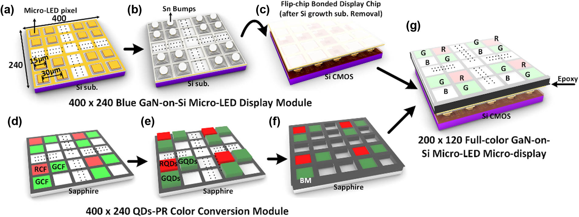
Figure 1 schematically presents the process flow of the full-color scheme of this monolithic GaN-on-Si micro-LED microdisplay. For the blue GaN-on-Si micro-LED display module, commercially available 4-in. (1 in. = 2.54 cm) GaN-on-Si LED epiwafers are used for the fabrication of self-emissive micro-LED arrays. Detailed process steps and conditions of the GaN-on-Si micro-LED display module were described in our previous work [37]. Several key steps are depicted in Figs. 1(a)–1(c), including mesa size definition, passivation, Sn microbumps thermal reflow, Au-Sn solder bonding, and Si growth substrate removal.
Figure 1.Process flow of the full-color GaN-on-Si micro-LED microdisplay. Schematic of the blue GaN-on-Si micro-LED module (a) after p- and n-electrode deposition, (b) after passivation, planarization, and Sn reflow, (c) flip-chip bonding. Schematic of the color conversion module, (d) after the color filter array (CFA) definition, (e) after QDs-PR patterning, and (f) after the second layer of black matrix (BM) isolation. (g) Schematic of the full-color GaN-on-Si micro-LED microdisplay.
The process inspections of the blue GaN-on-Si micro-LED display module are shown in Fig. 2. Figure 2(a) presents the as-fabricated micro-LED array on 4-in. GaN-on-Si epiwafers. This process can be scaled up following the size of the Si growth substrate. Each die of the micro-LED array occupies an area of , consisting of the p- and n-metal pad regions, which are arranged at the center and perimeter of the die, respectively. The well-shaped Sn microbumps are formed after thermal reflow and distributed uniformly across the array [Fig. 2(b)]. The heights of the Sn microbumps on p- and n-metal pads are 9 μm and 7 μm, respectively, resulting from the different sizes of the metal pads. The satisfied heights partially compensate GaN wafer curvature to ensure a high flip-chip bonding yield. With the GaN-on-Si micro-LED array bonded onto the complementary metal-oxide semiconductor (CMOS) backplane and Si growth substrate removal, a fully Au-Sn bonded and crack-free GaN thin film was exposed [Figs. 2(c) and 2(d)]. We define the voltage as pixel forward voltage when the driving current reaches 2.6 μA, corresponding to the current density of . Current-voltage () curves of 80 pixels randomly distributed in the array were measured, presenting a low reverse saturation current of 4.6 pA at and uniform forward voltage of which the variation is only 0.1 V [Fig. 3(a)]. As a result, the emission of each micro-LED pixel is fairly uniform across the array, which will not cause issues towards the color uniformity of color conversion for the full-color display. The whole display panel was fully lit up by directly powering the common p and n electrodes on the driver with a total injection current of 250 mA [Fig. 3(b)]. An enlarged view of the 15-μm pixel under the microscope indicates the uniform emission of the display panel at the pixel level. Few dead pixels are mainly caused by the reflow failure of Sn microbumps as well as the equipment limitation of our flip-chip bonder. The emission peak wavelength was measured as 440 nm by using an integrating sphere. Blue monochromatic images in vivid detail with a resolution of were clearly demonstrated using a commercial field-programmable gate array (FPGA) control board [Fig. 3(c)].
Figure 2.Fabrication of the monolithic blue GaN-on-Si micro-LED display module. (a) As-fabricated micro-LED array on the 4-in. GaN-on-Si epiwafer. Inspections of (b) the micro-LED array after Sn reflow, (c) flip-chip bonded blue display chip before and after the Si growth substrate removal. (d) Crack-free GaN surface after Si removal.
Figure 3.Characterization and demonstration of the monolithic blue GaN-on-Si micro-LED display. (a) curves of 80 pixels randomly picked from the single die of the micro-LED array. (b) Image of the micro-LED display chip fully powered on with injection current of 250 mA (the inset is the electroluminance spectrum with dominant wavelength at 440 nm) and corresponding zoomed-in view of pixels. (c) The 4-bit grayscale displayed images.
Similar to the fabrication method of the micro-LED array, the standard photolithography process used in the traditional microelectronics industry was used for the fabrication of the color conversion module. The process flow is presented in Figs. 1(d)–1(f) and summarized below. To begin with, the first layer of the black matrix (BM) with red and green color filters (R/G CFs) was patterned successively. A Bayer CF array, including one red, one blue, and two green subpixels, was formed on the substrate [Fig. 1(d)]. After hard baking of the BM and CF, R/G QDs-PR was spin coated and patterned on top following the positions of R/G CFs [Fig. 1(e)]. The BM was patterned for the second time to fully isolate each subpixel [Fig. 1(f)]. Finally, the color conversion module was pixel to pixel aligned and laminated onto the exposed display area of the blue GaN-on-Si micro-LED display module through adhesive bonding [Fig. 1(g)]. Process inspections of the QDs-PR color conversion module are shown in Fig. 4. Codesigning with the blue GaN-on-Si display module, here we demonstrated the as-fabricated QDs-PR color conversion layer on a 4-in. double-polished 200-μm-thick sapphire substrate [Fig. 4(a)]. The area of each die keeps the same as the display area of the GaN-on-Si micro-LED chip, which is . Figure 4(b) demonstrates the scanning electron microscopy images of the color conversion layer before and after the second layer of BM patterning. The size of R/G QDs-PR patterns deviated from the designed 24 μm to 27 μm [Fig. 4(b1)] due to the minor overexposure of QDs-PR. The blue subpixel is intentionally left empty without patterning. With the second layer of BM passivation [Fig. 4(b2)], the opening of the BM is smaller than the size of QDs-PR, thus, fully isolating the subpixels and eliminating optical crosstalk in the color conversion layer due to the omnidirectional emission of QDs-PR. The thickness of the QDs-PR layer has to be well considered by compromising the color conversion efficiency and lithography condition of QDs-PR. In a certain thickness range, a thicker QDs-PR layer leads to higher conversion efficiency. However, the lithography condition of QDs-PR will be much more critical, resulting in a serious distortion of pattern due to overexposure. Here, 7 μm was selected as the optimized pattern thickness. The total thicknesses of R/G QDs-PR with R/G CFs are around 9 μm and 8 μm [Fig. 4(b3)], respectively. Considering the thickness difference of R/G CFs, the R/G QDs-PR thickness is around 7.5 μm and 6.5 μm. Figure 4(c) presents the clear RGGB subpixel arrangement under the illumination of UV light. UV epoxy curing was performed during the assembling process of the color conversion module and the blue GaN-on-Si micro-LED display module by the flip-chip bonder [Fig. 4(d)].
Figure 4.Fabrication of the monolithic QDs-PR color conversion module. (a) The as-fabricated QDs-PR color conversion module on the 4-in. sapphire substrate. (b) The scanning electron microscopy (SEM) images of color conversion layer (b1) after R/G QDs-PR patterning, (b2) after the second layer of BM isolation, and (b3) the cross section of the QDs-PR color conversion layer. (c) Inspection of the QDs-PR color conversion module under UV excitation and zoomed-in view of RGGB subpixel arrangement. (d) Assembling of the blue GaN-on-Si micro-LED display module and color conversion module through adhesive bonding.
The color conversion properties of QDs-PR applied in the color conversion module were measured and analyzed by a 300-μm blue standard LED fabricated on the same epiwafer. The 7-μm-thick R/G QDs-PR layers were separately prepared on two pieces of thin glass by spin coating. Figure 5(a) shows the spectra of the standard LED driven at different current densities. The inset is the reference LED powered at a current density of . The excited spectra of the GQDs-PR and RQDs-PR layers illuminated by the standard LED are plotted in Figs. 5(b) and 5(c) in which the peak wavelength of converted green and red is 530 nm and 640 nm, respectively. To characterize the absorption and conversion properties of the QDs-PR, here we divided the total light output power (LOP) calculated from the spectra into three parts in which the blue part corresponds to power integrated from 400 nm to 500 nm, and the green and red parts correspond to the integral interval at [500 nm, 570 nm] and [580 nm, 720 nm], respectively. Therefore, the blue part represents the total pump power for the standard LED and unabsorbed power for QDs-PR. The green (red) part represents the converted power. The absorption ratio (Abr), conversion ratio (Conr), and efficiency () in terms of power can be expressed as
Figure 5.Characterizations of the QDs-PR thin film. (a) Spectra of the 300-μm standard blue LED powered at different current densities (the inset is the image of the blue reference LED powered at 20 mA). Spectra of the 7-μm-thick (b) GQDs-PR, (c) RQDs-PR illuminated by the blue LED under different current densities (the inset is the image of GQDs-PR/RQDs-PR illuminated by the blue LED powered at 20 mA). (d) Conversion ratio of 7-μm-thick R/G QDs-PR, (e) absorption ratio of 1.8-μm-thick RCF, 1.2-μm-thick GCF, and 7-μm-thick R/G QDs-PR, and (f) efficiency of 7-μm-thick R/G QDs-PR.
The relationship of Abr, Conr, and of R/G QDs-PR versus current density is plotted [Figs. 5(d)–5(f)]. At a current density of , which is the approximate operating current density of the micro-LED pixel in the display, the conversion ratio is around 50% and 34% for GQDs-PR and RQDs-PR, respectively. The conversion ratio shows a decreasing trend with the increase in current density. This might be due to the degradation of the quantum yield of QDs-PR at a strong light intensity, which increases the heat generation and degrades the performance of QDs inside. Quantum yield was estimated by integrating the number of photons instead of power, calculated as 60% and 51% for GQDs-PR and RQDs-PR, respectively. Conversion ratio or quantum yield describes the ability of how much light can be converted from the absorbed pump light for specific QDs, affecting the luminance of the full-color display. The absorption ratio, which is around 97% for RQDs-PR and 73% for GQDs-PR, significantly influences the color purity of the display, exhibiting independence from the intensity of pumping light and remaining almost the same over the current densities from 1 to . The efficiency is expressed as the product of the absorption ratio and conversion ratio. For 7-μm-thick GQDs-PR and RQDs-PR layer, is 36% and 33%, respectively. The maximum color gamut was estimated to be as low as 50.3% of the sRGB in the ideal case assuming that the crosstalk in the display is ignored, owing to a large amount of unabsorbed blue pump light, especially for the GQDs-PR. To filter the unabsorbed light, color filters were additionally applied with the QDs-PR layer. The absorbance and transmittance of 1.2-μm-thick GCF and 1.8-μm-thick RCF were measured and plotted in Fig. 6(a). Around 90% of transmittance is obtained both for RCF and for GCF. The excited spectra of R/G QDs-PR with R/G CFs were measured and shown in Figs. 6(b) and 6(c), respectively. It becomes apparent that the unabsorbed blue light is decreased both for GQDs-PR and for RQDs-PR due to the filtering of CF. Corresponding coordinates of green and red in CIE 1931 space are moved from (0.175, 0.316) and (0.197, 0.536) to (0.583,0.251) and (0.680,0.295), respectively. The maximum achievable color gamut was, therefore, estimated to increase from 50.3% to 113.3% of the sRGB, significantly improving the color performance of the QDs-PR color conversion layer. Compared to RQDs-PR, the GQDs-PR film is the main factor that limits the color performance of the display due to the limited absorption of GQDs-PR and GCF in the blue spectral region around 440–450 nm. The relationship of the color conversion film between green color purity and unabsorbed blue light has been studied in Ref. [39]. As a result, to obtain an acceptable purity of green, the power of converted green should, at least, be times larger than unabsorbed blue after the filtering of the CF. This corresponds to the color gamut of of the sRGB assuming the coordinate of red in CIE 1931 space is near the sRGB red.
Figure 6.Characterizations of CF, BM, and of the QDs-PR thin film after CF coating. (a) Transmittance and absorbance of 1.2-μm-thick GCF, 1.8-μm-thick RCF, and 1-μm-thick BM. Spectra of the 7-μm-thick, (b) GQDs-PR with GCF, and (c) RQDs-PR with RCF excited by the blue LED under different current densities. (The inset is the shift of green/red coordinate in CIE 1931 diagram.)
By integrating the blue GaN-on-Si display module and the QDs-PR color conversion module, a 4-bit grayscale full-color micro-LED microdisplay was achieved. Images with a resolution of presented in the blue monochromatic display shown in Fig. 4(c) were compressed and rearranged into RGGB format. Figure 7 demonstrates the full-color images in rich detail under the 3D microscope. RGB colors in the images are markedly reproduced, and color mixing is achieved by tuning the grayscale () of the blue pixels that correspond to the RGB subpixels. Only a few dead pixels, which were attributed to the process contamination of QDs-PR patterning and critical conditions of flip-chip bonding, were observed from the microscope. The maximum brightness of the full-color display is higher than 500 nits under the full-load condition.
Figure 7.The 4-bit full-color images demonstrated on the monolithically integrated full-color GaN-on-Si micro-LED microdisplay (demo videos see Visualization 1 and Visualization 2).
To estimate the color performance of the full-color microdisplay, RGB subpixels were turned on, respectively, and the emission spectra of these three cases were measured separately using spectroradiometers. Figure 8 shows the RGB monochromatic images of the display in an indoor lighting environment and their corresponding views from the microscope. Due to the limitation of the detection area of the spectroradiometers, we further divided the whole display panel into blocks, each of which consisted of subpixels. The spectrum of the RGB monochromatic display at each block was identified from 0 to 27. Therefore, the distribution of crosstalk between the subpixels in this full-color GaN-on-Si micro-LED microdisplay can be analyzed as follows.
Figure 8.Monochromatic blue, green, and red displayed images and corresponding view under a microscope.
We first discussed the possible sources that result in the crosstalk between RGB subpixels. In previous reported full-color micro-LED displays [24,40] which adopt the mass-transfer method to fabricate the blue micro-LEDs backlight on sapphire, the optical crosstalk effect is considered for the micro-LEDs backlight with a large pixel pitch as well as the gap between the micro-LED pixel and the color conversion layer. Different from the mass-transferred micro-LEDs backlight, our backlight display module is a thin-film display only consisting of an n-GaN and Al(Ga)N transition buffer layer with a total thickness of 2.4 μm. The whole micro-LED array can be regarded as a “single LED” consisting of micro-LED pixels since all of the micro-LED pixels in this thin-film display share the same n electrode. Because of the small pixel pitch and nonfully isolated structure of the micro-LED array, the optical crosstalk issue existing in the thin-film display needs to be taken into account especially when the pixel density further increases. As presented in Fig. 2(d), the light emitting downwards will be reflected by the p-metal stack and then go upwards. If the incident angles of upwards light rays are smaller than the critical angle, the light escapes from the top surface of Al(Ga)N buffer layer. Otherwise, total internal reflection occurs, and light keeps channeling in the n-GaN and Al(Ga)N buffer layers until emitting from the edge of the display. During this process, a small amount of light scatters at the top surface of the Al(Ga)N buffer layer due to the surface roughness, and some part of the light is reflected by the p-metal stack and then refracted at mesa sidewalls [Fig. 9(a)]. The crosstalk light existing in the micro-LED array acts as the blue light leakage to those unaddressed pixels, thus, influencing the color performance of full-color display if we further integrate the QDs-PR color conversion module on top. By calculating the light intensity distribution of Fig. 9(a), we estimate the power percentage of the blue leakage light at the nearest-neighboring unaddressed pixel as around 0.5%. Besides the crosstalk in the GaN-on-Si backlight display module, the assembling of the backlight display module and color conversion module introduces blue light leakage because of misalignment induced by the flip-chip bonder (4–6 μm). For such a small-size microdisplay, the gap between two modules is not the major factor since the color conversion module is directly laminated on the flat surface of the Al(Ga)N buffer layer. As presented in Fig. 9(b) when only green subpixels were turned on, both considerable red and blue peaks were observed on the green spectra. The reasons that cause the unexpected red and blue peaks are evidently different. For the red peaks on green spectra, RQDs-PR patterns were excited by the blue light leakage coming from the position of the green subpixels. As discussed above, this blue light leakage results from the micro-LED array in the GaN-on-Si backlight display module as well as the misalignment between the QDs-PR color conversion module and the backlight display module. Another possible source that contributes to the red peaks originates from the green light emitted by the GQDs-PR patterns in which green light transmits to the adjacent red subpixels through the isolated BM grid and pumps the RQDs-PR. To explore the crosstalk between subpixels in the QDs-PR layer, we measured the optical properties of the BM used in our experiments as shown in Fig. 6(a). The absorbance of the 1-μm-thick BM increases from 2.1 to 4.5 in the full wavelength region from 700 nm (red) to 400 nm (blue–violet). In this fully isolated QDs-PR color conversion layer, the second layer of the BM passivation is around 2–3 μm in thickness, which indicates that far less than 0.1% of blue (green) light can transfer through the BM and pump the adjacent subpixels. Therefore, the leakage path between subpixels in the QDs-PR color conversion module can be just ignored. Unlike the red peaks, the unexpected blue peaks on the green spectra come from the unabsorbed blue light from the GQDs-PR conversion layer itself as well as the blue leakage light at red and blue subpixels coming from the position of green subpixels. The source of crosstalk that contributes to the red spectra can be analyzed in the same manner as the green spectra discussed above. In the case of blue subpixels turned on only, we do observe that the green and red peaks are comparatively weak in the normalized spectra. This is due to the fact that most blue light directly comes out from the position of blue subpixels without the attenuation of QDs-PR conversion, while the leakage light transporting to the positions of adjacent red and green subpixels only accounts for a small portion of the total pumping light. Furthermore, the leakage light is, subsequently, absorbed and converted by the QDs-PR, of which conversion efficiency is relatively low, thus, producing the minimum effect of red/green crosstalk on the blue spectra.
Figure 9.The display panel was divided into 28 blocks numbered from 0 to 27, each of which includes subpixels. (a) The single pixel was addressed in the GaN-on-Si backlight display. (b) Display spectra of blocks 0–27 when blue, green, and red subpixels were turned on, respectively. (c) Schematic of the blue light leakage between RGB subpixels.
The angular dependence of the full-color microdisplay is measured using spectroradiometers, as shown in Fig. 11(a). Compared to the mass-transferred RGB micro-LED panel [41,42], which normally delivers a Lambertion shape emission, the red and green light from this monolithically integrated full-color micro-LED panel presents a radiation pattern between the omnidirectional and Lambertion shapes. In the range of viewing angles between , the angular distribution of R/G QDs-PR is closer to the isotropic shape. For the angles larger than in the normal direction of the display panel, the emission intensity decreases rapidly due to the isolation of the BM on the sidewall of R/G QDs-PR patterns. The weak light intensity is difficult to be detected due to the accuracy limitation of the measurement setup. Further optical devices, such as microlenses can be applied on top of the color conversion module to collimate emission beams and improve the light extraction efficiency in future AR/VR devices. Figure 11(b) presents the CIE 1931 diagram of this full-color microdisplay in which the (, ) coordinates of B, G, R are located at (0.162, 0.017), (0.218, 0.562), and (0.622, 0.329), respectively. The display color gamut is measured to be as wide as around 104% of the sRGB. Compared to our previous work [38], the color gamut has been significantly improved. It is especially noted that the green color is still not as good as the sRGB green (0.3, 0.6), which can be attributed to the relatively low efficiency of GQDs-PR as well as the more severe crosstalk caused by the blue leakage light as we discussed. A thicker QDs-PR layer and higher color conversion efficiency will both lead to higher display quality, but trade-offs between the process and the display quality, such as color gamut and luminance need to be taken into consideration.
Figure 11.Display color performance characterization. (a) Angular dependence of and (b) color gamut of this full-color micro-LED microdisplay.
The 4-in. GaN-on-Si blue LED epiwafer was bought from Enkris Semiconductor, Inc. The wafer was cleaned by the mixture and followed by aqua regia to remove the possible organic and metal particles before the process. The 115-nm indium tin oxide (ITO) was first deposited on p-GaN by e-beam evaporation. Then, the 15-μm mesa region was defined by photolithography using positive photoresist FD-6400. The unmasked ITO region was wet etched by diluted aqua regia (1:100) until a clear undercut can be seen. Before wet etching, the photoresist mask was baked at 110°C for 10 min to increase the adhesion with ITO to better control the undercut. Then, the mesa region was self-aligned to the ITO contact and formed by inductively coupled-plasma (ICP) etching with the 120°C hard-baked photoresist on top as the etching mask. Around 500 nm, the height mesa was etched. The wafer was dipped in the above diluted aqua regia solution for comparable time to remove the possible ITO particle on the mesa sidewall induced by ICP etching. Then, ITO was annealed at 600°C in atmosphere to form an ohmic contact with p-GaN by rapid thermal annealing. The Cr/Al/Au metal stack was deposited as individual-p and common-n electrodes. The common-n electrode was designed as a gridlike structure to improve the current spreading over the whole micro-LED array. A layer of (350 nm) was deposited by plasma-enhanced chemical vapor deposition to prevent the squeezed-out Sn from flowing on the sidewall during flip-chip bonding as well as passivating the sidewall. Contact holes (9 μm) were then opened on p-metal electrodes for the Sn microbumps connection. The transparent everlight overcoat photoresist was spin coated on the wafer for planarization to assist Sn reflow. Finally, 2-μm-thick thermal-evaporated Sn-metal pads were deposited on individual Sn-metal pads by lift-off. The Sn-metal pads were reflowed into Sn microbumps at 240°C with the help of Alpha Flux, which can be washed away by de-ionized water and acetone. Then, the micro-LED array was flip chip bonded onto the Si CMOS driver (co-designed by our group and HKUST colleagues) at 220°C for 5 min with formic acid gas via the Au-Sn interface (Au on the driver side and Sn on the micro-LED array side). The bonded chip was then thinned from 800 μm down to 100 μm on the Si growth substrate side and protected by an antiacid polymer to remove the remaining Si substrate by the hexitol nucleic acids-mixed solution () until the crack-free GaN surface was exposed.
B. Color Conversion Module Fabrication
A 4-in. sapphire substrate was utilized as a carrier for the fabrication of the QDs-PR color conversion module. The sapphire substrate was first thinned down to 200 μm, polished on the double side, and cleaned by IPA. Commercially available colloidal CdSe/ZnS (core/shell) R/G QDs combined with the photoresist were utilized in this paper. A layer of 1-μm-thick BM grid was spin coated on the sapphire at a speed of 500 r/min for 2 min to define the pixel arrangement; then hard baked at 250°C for 30 min to prevent it from being dissolved by the followed color filters or QDs-PR. The 1.2-μm-thick GCF and 1.8-μm-thick RCF were obtained by spin coating at a speed of 500 r/min for 2 min and then patterned into pixels with a size of μμ, respectively. Between each layer of CF patterning, the wafer was also hard baked at 250°C for 30 min. Then, the 6.5-μm-thick GQDs-PR layer was spin coated on the CFA at a speed of 300 r/min for 2 min and patterned into pixels with sizes of μμ exactly following the position of GCF. The GQDs-PR color conversion layer was cured under a UV light with a peak wavelength of 405 nm for separated 6 min. Similarly, using the same spin-coating conditions as GQDs-PR, the 7.5-μm-thick RQDs-PR layer was obtained with pixel sizes of μμ by photolithography. Another 6 min of UV light irradiation was used to cure the RQDs-PR. Finally, the last layer of the BM was spin coated and patterned to fully isolate and cover the sidewall of QDs-PR to eliminate the crosstalk between the color conversion layers. The size of the last layer of the BM opening is μμ.
C. Two Modules Integration and Characterization
The blue GaN-on-Si display module was wire-bonded to a daughterboard and connected to an FPGA board through a flexible flat cable. Full-color images and videos were decoded into the binary format by MATLAB and read by the FPGA board. The GaN-on-Si display module and the color conversion module were integrated using adhesive bonding by applying a thin layer of UV epoxy on the GaN-on-Si display module side. The bonding force applied on the color conversion module side was 20 N. Epoxy was meanwhile cured by UV irradiation during the bonding process. curves of micro-LED pixels were measured by the HP4516 semiconductor parameters analyzer. Photographs in the view of pixels and the whole display were captured by a Moticam 1080 CMOS camera and Xiaomi smartphones, respectively. The optical properties of the QDs-PR thin film were characterized by Ocean Optics USB-2000 spectrometers with an integrating sphere. The spectra-, brightness-, and angular-dependent emissions of the full-color display panel were measured by a spectroradiometer (Photoresearch PR-655 SpectraScan).
4. CONCLUSIONS
In conclusion, we demonstrated a practical monolithically integrated full-color micro-LED microdisplay with a resolution of 423 ppi through the integration of a blue GaN-on-Si display module and QDs-PR color conversion module. The monolithic blue GaN-on-Si micro-LED display was achieved using standard 4-in. blue GaN-on-Si epiwafers of which the dominant wavelength was 440 nm for the fabrication of micro-LED arrays and flip chip bonded with a custom-designed CMOS driver. The color conversion module with a Bayer matrix configuration was monolithically fabricated using QDs-PR and CF patternings on a 4-in. thinned-down and polished sapphire substrate. Two modules were aligned pixel to pixel and integrated through adhesive bonding. The absorption and conversion properties of the optimized-thickness QDs-PR layer were explored under different current densities of the blue-pumping LED. To overcome the issue of inefficient absorption of QDs-PR, CFA was applied with the QDs-PR color conversion layer to filter the unabsorbed light, consequently, improving the purity of the converted color. The crosstalk issue caused by the blue light leakage resulting from the misalignment of the two modules’ integration and crosstalk in the bottom the GaN-on-Si backlight display was discussed. The distribution of the light leakage was overall uniform and analyzed across the whole display panel. The percentages of the efficient pumping light for the blue, green, and red subpixels were around 95%, 89%, and 92%, respectively. The color gamut of this full-color micro-LED microdisplay was as large as 104% of the sRGB, and the luminance was larger than 500 nits under the full-load condition of the driver. In our previous demonstration of a monolithic blue GaN-on-Si display, the maximum brightness of 8300 nits can be achieved. Therefore, future improvements on the full-color microdisplay require the optimization of QDs-PR both from the aspect of absorption and conversion properties to increase the display luminance and color gamut. The crosstalk issue induced by the blue leakage light can be minimized by fully isolating the Al(Ga)N buffer layer of the bottom GaN-on-Si micro-LED display during the micro-LED array fabrication as well as the improvement in equipment alignment accuracy. The QDs-PR color conversion module necessitated a more uniform profile of R/G QDs-PR patterns to reduce the variations in color purity for both pixel level and display level. The full-color micro-LED microdisplay we demonstrated here proves the feasibility of large-scale manufacturing through parallel integration of the QDs-PR color conversion module and the GaN-on-Si micro-LED display module, also providing the possibility for further performance enhancement.
Acknowledgment
Acknowledgment. The authors would like to thank the NFF and Epack of HKUST for technical support.
[3] Y. Huang, E.-L. Hsiang, M.-Y. Deng, S.-T. Wu. Mini-LED, micro-LED and OLED displays: present status and future perspectives. Light Sci. Appl., 9, 105(2020).
[4] W. C. Chong, W. K. Cho, Z. J. Liu, C. H. Wang, K. M. Lau. 1700 pixels per inch (PPI) passive-matrix micro-LED display powered by ASIC. IEEE Compound Semiconductor Integrated Circuit Symposium, 1-4(2014).