Ren-Yan WANG, Lin GAN, Tian-You ZHAI, [in Chinese], [in Chinese], [in Chinese]. ReX2 (X=S, Se): A New Opportunity for Development of Two-dimensional Anisotropic Materials[J]. Journal of Inorganic Materials, 2019, 34(1): 1
Search by keywords or author
- Journal of Inorganic Materials
- Vol. 34, Issue 1, 1 (2019)
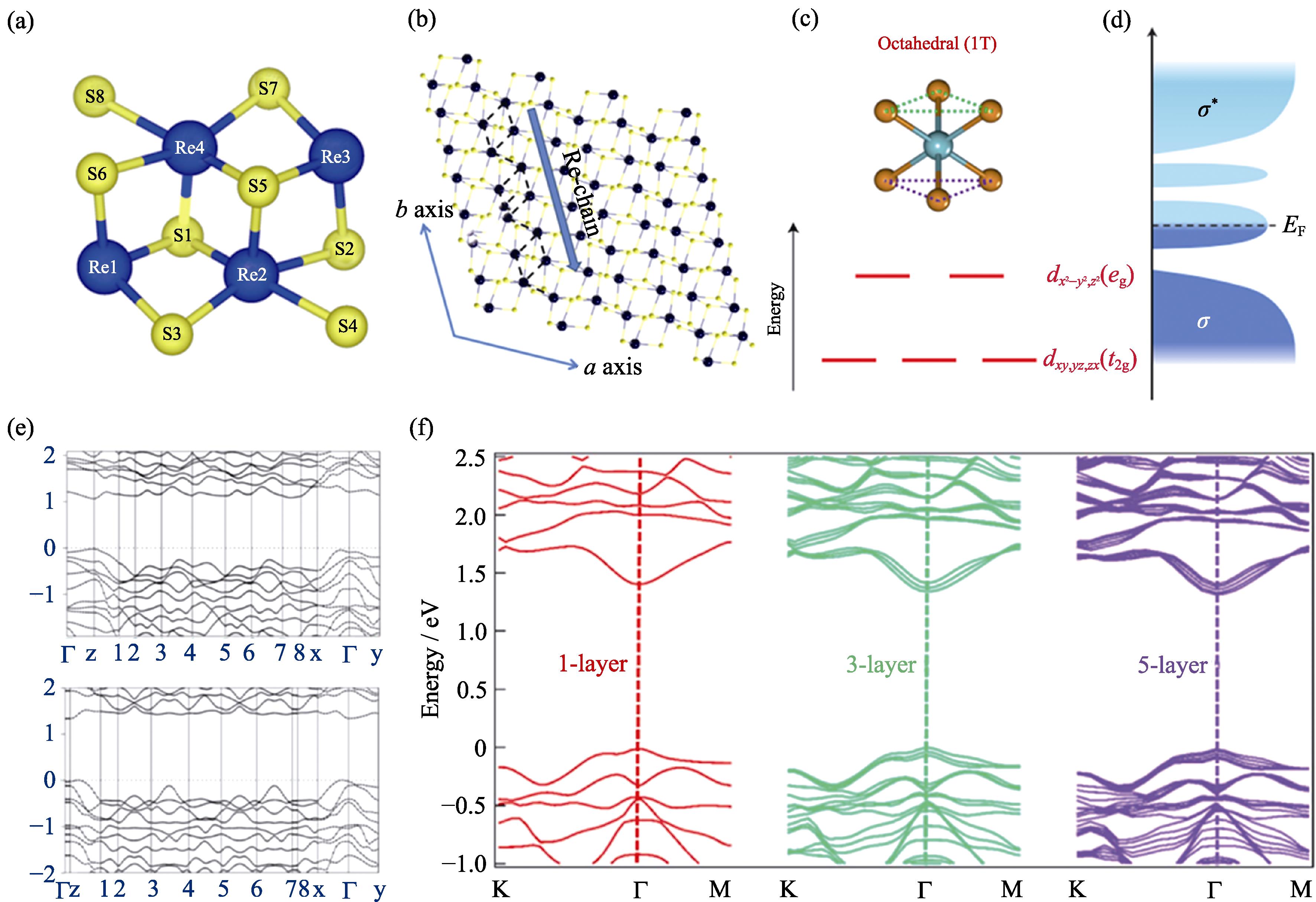
![(a) The model unitcell view of ReS2[33]; (b) Top view of the crystalline structure of distorted-1T phase of monolayer ReX2(Black balls represent Re atoms and yellow balls represent S or Se atoms); (c, d) Schematic images of 1T lattice symmetries and energy levels of d-orbital electrons induced by the crystal field[39,40]; (e) First-principles scalar relativistic projector augmented wave calculations of electronic band structures for bulk (top) and single-layer (down) ReSe2[50]; (f) Band structure of monolayer, trilayer and five-layer ReS2 by ab initio-calculations[51]](/richHtml/jim/2019/34/1/1/img_1.png)
. (a) The model unitcell view of ReS2[33]; (b) Top view of the crystalline structure of distorted-1T phase of monolayer ReX2(Black balls represent Re atoms and yellow balls represent S or Se atoms); (c, d) Schematic images of 1T lattice symmetries and energy levels of d-orbital electrons induced by the crystal field[39,40]; (e) First-principles scalar relativistic projector augmented wave calculations of electronic band structures for bulk (top) and single-layer (down) ReSe2[50]; (f) Band structure of monolayer, trilayer and five-layer ReS2 by ab initio-calculations[51]
![PL spectra of ReS2 flakes with different number of layers; (b) Integrated PL intensity as a function of number of layers (normalized to that of monolayer) in ReS2, MoS2, MoSe2, WS2 and WSe2[50]; Raman spectra recorded on (c) N-layer ReS2 and (d) N-layer ReSe2 in the parallel polarization configuration[58]; (e) Schematic for the process of oriented self assembly of ReS2 nanoscrolls[59]; (f) Schematic for the TIB of a single ReS2 nanowall[60]](/richHtml/jim/2019/34/1/1/img_2.png)
. PL spectra of ReS2 flakes with different number of layers; (b) Integrated PL intensity as a function of number of layers (normalized to that of monolayer) in ReS2, MoS2, MoSe2, WS2 and WSe2[50]; Raman spectra recorded on (c) N-layer ReS2 and (d) N-layer ReSe2 in the parallel polarization configuration[58]; (e) Schematic for the process of oriented self assembly of ReS2 nanoscrolls[59]; (f) Schematic for the TIB of a single ReS2 nanowall[60]
. (a) SEM image of ReS2 powders and TEM image of as-exfoliated ReS2 nanosheets with inset showing photograph of a typical dark-brown exfoliated ReS2 suspension in water; (b) High-resolution STEM image of as-exfoliated ReS2 nanosheets[70]; (c) Schematics for different density gradient ultracentrifugation ReS2 nanosheets through iDGU; (d) Atomic force microscopy image of solution-processed ReS2 following deposition on a Si wafer; (e) Raman spectrum of ReS2 nanosheets[63]
. (a) Schematic diagram of synthesized ReS2 film by PVD; (b) Raman spectrum of ReS2 film ; (c) Optical photograph of grown ReS2 film on the SiO2/Si substrate with inset showing the AFM and TEM images[88]; (d) A picture of bare and as-grown ReS2 bilayer film on sapphire wafer by CVD; (e) Optical microscope image of the ReS2 hexagons[74]
. (a) Schematic for the tellurium-assisted CVD growth approach; (b) Optical image of ReS2 after transferred onto SiO2/Si (300 nm) substrate with inset showing AFM image of ReS2 on mica substrate[77]; (c) Schematic of the CVD growth of ReSe2 in the confined reaction space and the surface reaction during the epitaxial growth of the ReSe2 atomic layer on mica; (d) Optical image of ReSe2 in A and B face[89]
. (a) A schematic illustrating the pump-probe experiment of few-layer ReS2 with inset showing optical image of few-layer ReS2; (b) Polarization-dependent absorption spectra of few-layer ReS2; (c) Corresponding spectral weights of Lorentzian contributions of X1 (blue dots) and X2(red dots). Yellow line represents the b -axis[122]; (d) Raman spectrum for bulk ReS2[128] and Low-frequency Raman spectroscopy of few layer ReS2[131]; (e) Unpolarized Raman spectra as a function of sample orientation angle; (f) High-magnification ADF-STEM image and corresponded polarization-and orientation-resolved Raman spectra[130]
. (a) Optical microscope image of ReS2 four probe transistor; (b) The magnified ADF images taken from the sample in (a); (c) The direction-dependent I -V characteristics with inset showing nonlinear I -V behavior indicate the Schottky Au/ReS2 contacts; (d) The direction-dependent transfer characteristics[137]; (e) Transfer curves of anisotropic ReS2 FETs along two sides with top inset showing optical image of the devices (Scale bar, 10 μm) and low inset showing the 4-probe resistance of the same devices. (f) Normalized field-effect mobility of a six-layer device with inset showing the optical image of the device[51]; (g) Angle-dependent transfer curves of ReS1.23Se0.77 alloy device with inset showing optical image of ReS2 device[76]
. (a) The photocurrent of ReS2 change as a function of drain bias under different polarization light illuminations; (b) The change of the photocurrent under different drain biases plotted as a function of polarization angle[112]; (c) Photocurrent response of ReS1.06Se0.94 alloy device under light on and off irradiation, and under light with different polarization direction; (d) Polar plots for the photocurrent with respect to the polarization angle of the incident light[76]; (e) Schematic structure of ReSe2 photodetectors; (f) The SEM image and polarization-dependent photocurrent mapping of the device[15]
. (a) Optical microscopy image of an exfoliated ReS2 ?ake; (b) Through-plane TDTR data at two modulation frequencies; (c) In-plane TDTR data at f = 1.1 MHz and time delay of -50 ps. The dashed lines are the intensity profile of the laser beam; (d) 2D beam-offset scan of the TDTR signal; (e) In-plane thermal conductivity of exfoliated ReS2 ?akes as a function of thickness[151]
|
|
Table 2. The 18 Raman active frequencies in bulk and monolayer ReS2 under 633 nm solid state laser excitation[35]

Set citation alerts for the article
Please enter your email address


