
Liangchuang Su, Tao Chen. Wireless Stimulation System with Multiple Channels and Independent Regulation for Optogenetics in Vitro[J]. Laser & Optoelectronics Progress, 2021, 58(19): 1917001
- Laser & Optoelectronics Progress
- Vol. 58, Issue 19, 1917001 (2021)
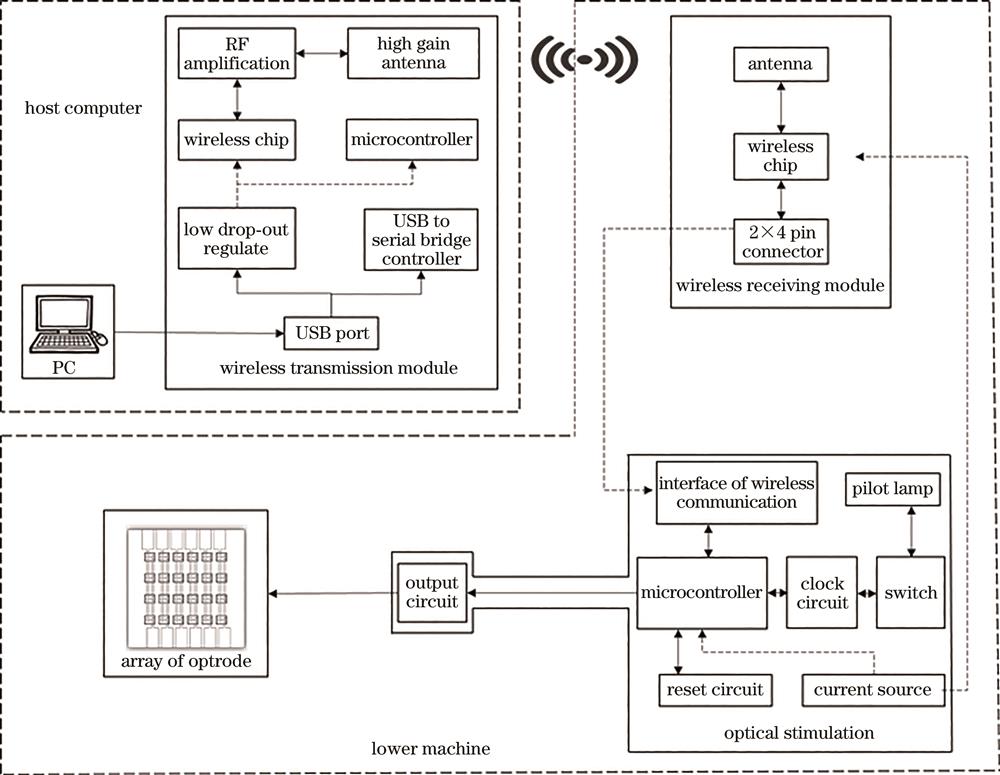
Fig. 1. Schematic representation of the structure of optical stimulation system
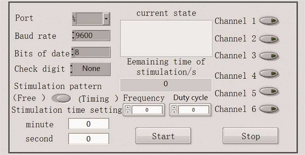
Fig. 2. Software interface of the host computer
Fig. 3. Photo of baseplate of optrode
Fig. 4. Welding process of
Fig. 5. Flowchart of program of stimulator
Fig. 6. Photograph of optical stimulator and optrode
Fig. 7. Relationship between output optical power and distance and the number of open channel. (a) Relationship between output optical power and distance; (b) relationship between output optical power and the number of open channel
Fig. 8. Relationship between output optical power and running time
Fig. 9. Output waveforms of stimulator under different standard frequency values. (a) 1 Hz; (b) 50 Hz; (c) 250 Hz; (d) 500 Hz
Fig. 10. Relationship between standard frequency and output frequency or error
Fig. 11. Relationship between packet loss rate and distance of wireless communication
Fig. 12. Testing of multichannel of optrode. (a) Channel 1 is open; (b) channel 2 is open; (c) channel 3 is open; (d) channel 4 is open; (e) channel 5 is open; (f) channel 6 is open; (g) channels 1,3,and 5 are open; (h) channels 2, 4, and 6 are open; (i) all channels are open
|
Table 1. Parameters of D2227 chip

Set citation alerts for the article
Please enter your email address
© Copyright 2018-2021 | Chinese Laser Press. All Rights Reserved 沪ICP备15018463号-20