
Xianhe Liu, Yi Sun, Yakshita Malhotra, Ayush Pandey, Ping Wang, Yuanpeng Wu, Kai Sun, Zetian Mi. N-polar InGaN nanowires: breaking the efficiency bottleneck of nano and micro LEDs[J]. Photonics Research, 2022, 10(2): 587
- Photonics Research
- Vol. 10, Issue 2, 587 (2022)
![Variations of peak EQE of InGaN/GaN LEDs versus lateral dimension for some reported devices in the literature, showing the significantly reduced efficiency with decreasing device size [1–19" target="_self" style="display: inline;">–19]. The current density corresponding to the peak EQE varies in the range of ∼1−26 A/cm2. Blue square: blue LEDs. Green square: green LEDs.](/richHtml/prj/2022/10/2/02000587/img_001.jpg)
Fig. 1. Variations of peak EQE of InGaN/GaN LEDs versus lateral dimension for some reported devices in the literature, showing the significantly reduced efficiency with decreasing device size [119" target="_self" style="display: inline;">19]. The current density corresponding to the peak EQE varies in the range of ∼ 1 − 26 A / cm 2
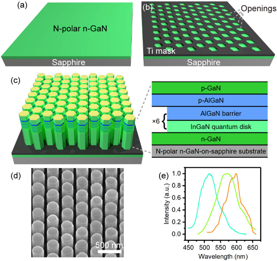
Fig. 2. (a) Schematic of a N-polar GaN template grown on sapphire substrate. (b) Schematic of a patterned N-polar n-GaN template on sapphire using Ti mask. (c) Schematic of InGaN/GaN nanowires formed by selective area epitaxy. Inset: schematic of the LED heterostructure. (d) Scanning electron microscopy (SEM) image of the nanowires. (e) Photoluminescence spectra measured from InGaN nanowires with various indium compositions in the quantum disk active region.
Fig. 3. (a) STEM-HAADF image of a single InGaN/AlGaN nanowire with six stacks of InGaN quantum disks exhibiting green emission. (b) High magnification of the region around the quantum disks. (c) Elemental mapping of In and Al in the region denoted by the blue box in (b). (d) The profile of Al distribution along the red dashed line in (b). (e) High-magnification STEM annular bright-field image showing the atomic stack order, where green circles represent Ga and red circles represent N.
Fig. 4. (a) I-V characteristics of a submicrometer InGaN nanowire LED. Inset: SEM image of the current injection window of the device. (b) Representative electroluminescence spectra of a N-polar submicrometer LED. Inset: optical microscopy image of the device.
Fig. 5. Variations of (a) output power and (b) EQE with current density.
Fig. 6. Left axis: IQE (solid blue curve) derived based on the ABC model analysis. The estimated IQE (blue circles) based on the measured EQE divided by the light extraction efficiency is also shown for comparison. Right axis: estimated contribution of AN C N 3 + D N 4 ∼ 89 %

Set citation alerts for the article
Please enter your email address
© Copyright 2018-2021 | Chinese Laser Press. All Rights Reserved 沪ICP备15018463号-20