• Acta Photonica Sinica
  • Vol. 49, Issue 8, 0823001 (2020)
Pei MA1, Hong-yun XIE1、*, Yin SHA1, Yang XIANG1, Liang CHEN2, Min GUO1, Xian-cheng LIU1, and Wan-rong ZHANG1
Author Affiliations
  • 1Faculty of Information Technology, Beijing University of Technology, Beijing 100124, China
  • 2College of Physics and Electronic Engineering, Taishan University, Taian, Shandong 271000, China
  • show less
    DOI: 10.3788/gzxb20204908.0823001 Cite this Article
    Pei MA, Hong-yun XIE, Yin SHA, Yang XIANG, Liang CHEN, Min GUO, Xian-cheng LIU, Wan-rong ZHANG. Effect of Optical Window on Optical Response Characteristics of SiGe/Si Heterojunction Phototransistor[J]. Acta Photonica Sinica, 2020, 49(8): 0823001 Copy Citation Text show less
    Schematic of the SiGe/Si HPT
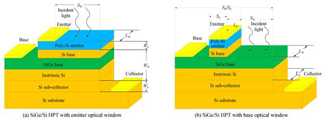
    Fig. 1. Schematic of the SiGe/Si HPT
    Current gain and characteristic frequency of corresponding SiGe/Si HBT
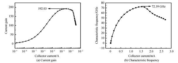
    Fig. 2. Current gain and characteristic frequency of corresponding SiGe/Si HBT
    Initial photogenerated current of SiGe/Si HPT with different optical window position
    Fig. 3. Initial photogenerated current of SiGe/Si HPT with different optical window position
    Current gain of SiGe/Si HPT with different optical window position
    Fig. 4. Current gain of SiGe/Si HPT with different optical window position
    Collector current of SiGe/Si HPT with different optical window position
    Fig. 5. Collector current of SiGe/Si HPT with different optical window position
    Optical gain of SiGe/Si HPT with different optical window position
    Fig. 6. Optical gain of SiGe/Si HPT with different optical window position
    Movement of photo-generated carriers with different optical window on base
    Fig. 7. Movement of photo-generated carriers with different optical window on base
    Optical characteristic frequency of SiGe/Si HPT with different optical window positions
    Fig. 8. Optical characteristic frequency of SiGe/Si HPT with different optical window positions
    Collector current of SiGe/Si HPT with different optical window areas
    Fig. 9. Collector current of SiGe/Si HPT with different optical window areas
    Optical gain of SiGe/Si HPT with different optical window areas
    Fig. 10. Optical gain of SiGe/Si HPT with different optical window areas
    Emitter junction capacitor and collector junction capacitor of SiGe/Si HPTs with different optical window areas
    Fig. 11. Emitter junction capacitor and collector junction capacitor of SiGe/Si HPTs with different optical window areas
    Optical characteristic frequency of SiGe/Si HPT with different optical window areas
    Fig. 12. Optical characteristic frequency of SiGe/Si HPT with different optical window areas
    ParameterPolysiliconemitterSi baseSi1-xGexbaseIntrinsic SibaseSi collectorSisub-collector
    Eg/eV1.121.120.941.121.121.12
    Affinity/eV4.054.054.174.054.054.05
    Permittivity11.7011.7012.7211.7011.7011.70
    Mun0/(cm2·V-1·s-1)1 4001 4001 4301 4001 4001 400
    Mup0/(cm2·V-1·s-1)500500480500500500
    Vsatn/(cm·s-1)1×1071×1071×1071×1071×1071×107
    Vsatp/(cm·s-1)1×1071×1071×1071×1071×1071×107
    Taun0/s1×1071×1073×1051×1071×1071×107
    Taup0/s1×1071×1071×1051×1071×1071×107
    Real.index3.633.633.743.633.633.63
    Imag.index0.0020.0020.0100.0020.0020.002
    Table 1. Material parameters used in the simulation model of SiGe/Si HPT
    Optical window positionsOptical window areasGoptmaxfToptmaxGopt·fTopt
    Emitter10 μm×10 μm9.2412.96119.75
    Base10 μm×10 μm1.5216.7525.460
    Emitter50 μm×10 μm26.67.53200.298
    Base50 μm×10 μm2.5413.0833.223
    Table 2. Optical gain, optical characteristic frequency, and Gopt·fTopt of HPT with different optical window positions
    Optical windowareasICsat(1.5 mW)Growth rate of saturatedcurrent per unit areaGoptGrowth rate of opticalgain per unit area
    3 μm×10 μm2.924.81
    5 μm×10 μm3.620.356.060.625
    10 μm×10 μm5.540.3849.240.636
    30 μm×10 μm10.520.24920.780.577
    50 μm×10 μm12.860.11726.600.291
    Table 3. Saturation current, growth rate of saturated current per unit area, optical gain and growth rate of optical gain per unit area of SiGe/Si HPT with different optical window areas
    Optical windowareasGoptmaxGrowth rate ofoptical gain perunit areafToptmax/GHzDecline rate offToptmax/(per unit area)Gopt·fToptGrowth rate ofGopt·fTopt per unitarea
    3 μm×10 μm4.8114.7971.13
    5 μm×10 μm6.060.62514.330.2386.847.855
    10 μm×10 μm9.240.63612.960.274119.756.582
    30 μm×10 μm20.780.5778.700.213180.793.052
    50 μm×10 μm26.600.2917.530.058 5200.2980.975 4
    Table 4. Optical gain, optical characteristic frequency, and Gopt·fTopt of SiGe/Si HPT with different optical window areas
    Pei MA, Hong-yun XIE, Yin SHA, Yang XIANG, Liang CHEN, Min GUO, Xian-cheng LIU, Wan-rong ZHANG. Effect of Optical Window on Optical Response Characteristics of SiGe/Si Heterojunction Phototransistor[J]. Acta Photonica Sinica, 2020, 49(8): 0823001
    Download Citation