
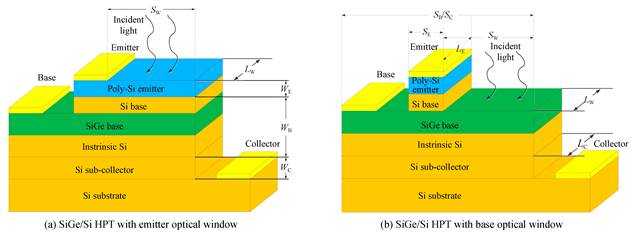
Pei MA, Hong-yun XIE, Yin SHA, Yang XIANG, Liang CHEN, Min GUO, Xian-cheng LIU, Wan-rong ZHANG. Effect of Optical Window on Optical Response Characteristics of SiGe/Si Heterojunction Phototransistor[J]. Acta Photonica Sinica, 2020, 49(8): 0823001
- Acta Photonica Sinica
- Vol. 49, Issue 8, 0823001 (2020)
Abstract


Set citation alerts for the article
Please enter your email address

© Copyright 2018-2021 | Chinese Laser Press. All Rights Reserved 沪ICP备15018463号-20