• Chinese Optics Letters
  • Vol. 13, Issue 3, 031401 (2015)
小波 李1, 永清 黄1、*, 俊 王1, 晓峰 段1, 瑞康 张2, 弘 李业1, 正 刘1, 琦 王1, 霞 张1, and 晓敏 任1、**
Author Affiliations
  • 1Institute of Information Photonics and Optical Communications, Beijing University of Posts and Telecommunications (BUPT); State Key Laboratory of Information Photonics and Optical Communications (BUPT), Beijing 100876, China
  • 2Key Laboratory of Semiconductor Materials Science, Institute of Semiconductors, Chinese Academy of Sciences, Beijing 100083, China
  • show less
    DOI: 10.3788/COL201513.031401 Cite this Article Set citation alerts
    小波 李, 永清 黄, 俊 王, 晓峰 段, 瑞康 张, 弘 李业, 正 刘, 琦 王, 霞 张, 晓敏 任. Metamorphic growth of 1.55  μm InGaAs/InGaAsP multiple quantum wells laser structures on GaAs substrates[J]. Chinese Optics Letters, 2015, 13(3): 031401 Copy Citation Text show less
    Structures schematic of laser epilayers and growth process on GaAs substrates.
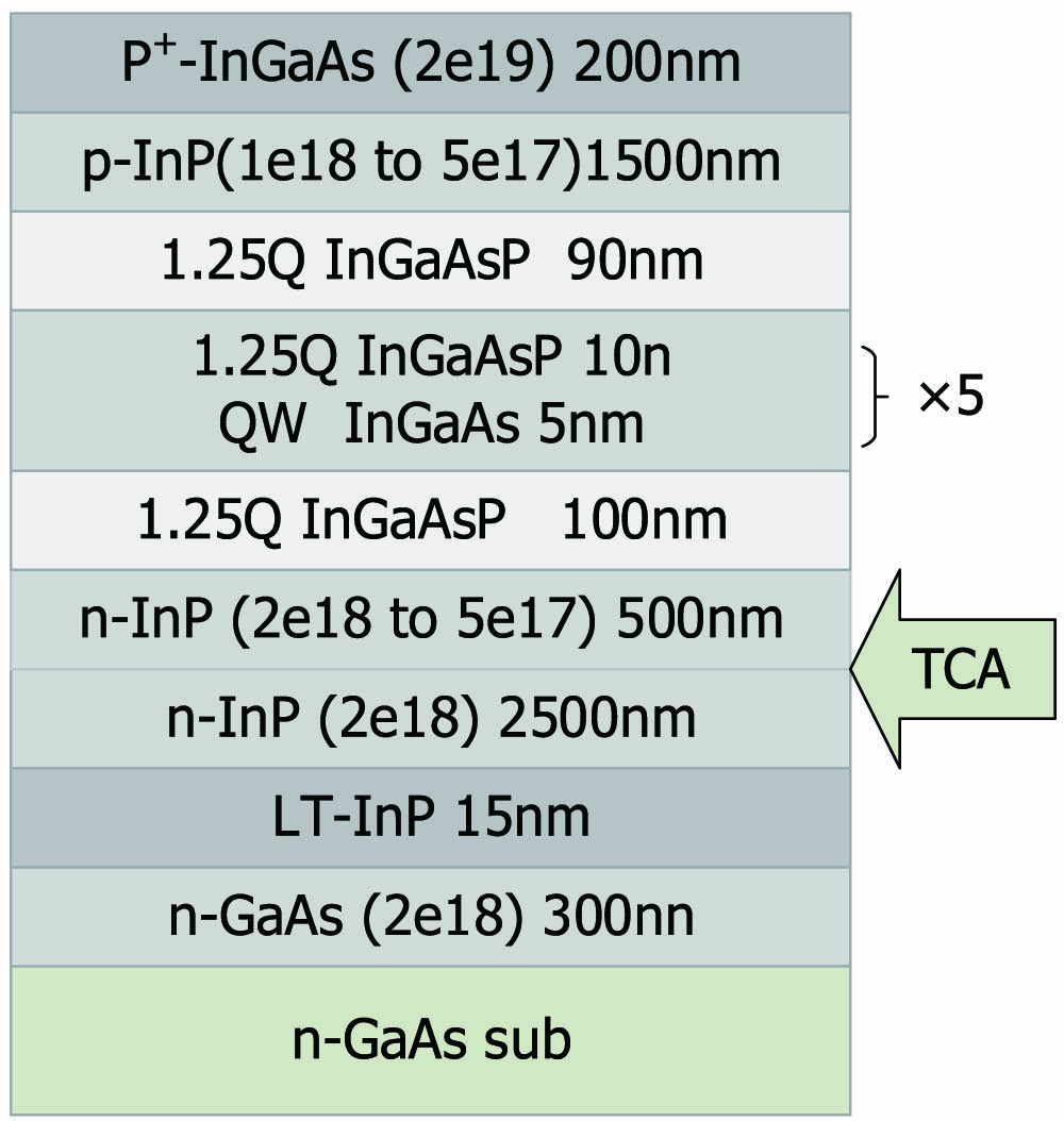
    Fig. 1. Structures schematic of laser epilayers and growth process on GaAs substrates.
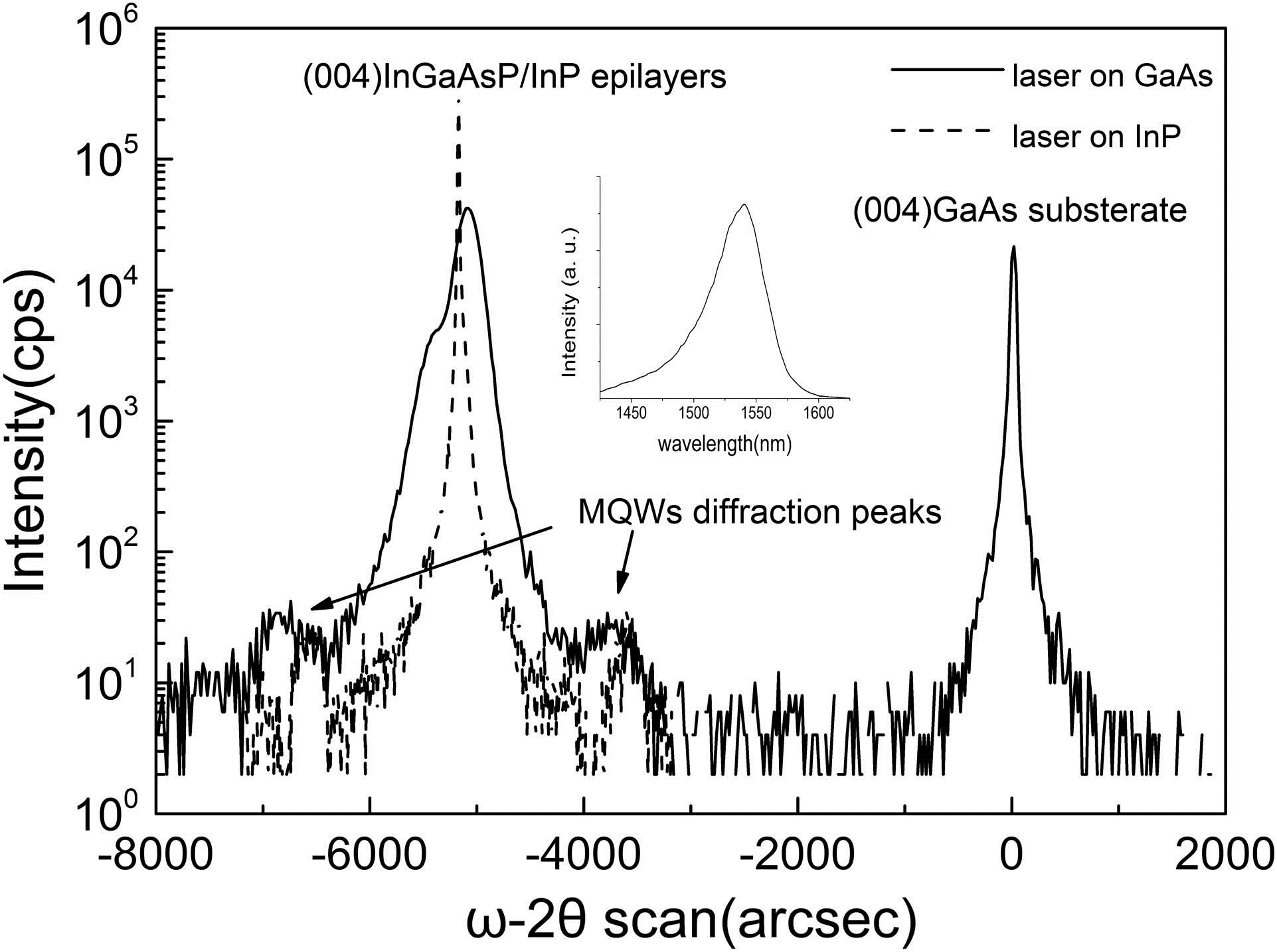
    Rocking curve (ω−2θ scan) of MQWs laser on GaAs substrate (solid line) and on InP substrate (dotted line) in the GaAs (004) reflection. Inset shows RT PL photoluminescence spectrum of MQWs for InP/GaAs laser after removing the surface layers.
    Fig. 2. Rocking curve (ω2θ scan) of MQWs laser on GaAs substrate (solid line) and on InP substrate (dotted line) in the GaAs (004) reflection. Inset shows RT PL photoluminescence spectrum of MQWs for InP/GaAs laser after removing the surface layers.
    Measured carrier concentration profiles of MQWs InP/GaAs laser material by ECV. Inset shows the hole concentration of p-type contact layer and part of cladding layer.
    Fig. 3. Measured carrier concentration profiles of MQWs InP/GaAs laser material by ECV. Inset shows the hole concentration of p-type contact layer and part of cladding layer.
    (a) Cross-sectional TEM images of epilayers on GaAs substrate; (b) TEM images of active regions and (c) TEM images of active regions with dislocations.
    Fig. 4. (a) Cross-sectional TEM images of epilayers on GaAs substrate; (b) TEM images of active regions and (c) TEM images of active regions with dislocations.
    (a) Schematic structures of the device with 50 μm strip. (b) A single emitter laser. Inset shows the individual chip of the laser diode.
    Fig. 5. (a) Schematic structures of the device with 50 μm strip. (b) A single emitter laser. Inset shows the individual chip of the laser diode.
    Typical curves of output power and voltage versus injection current for the emitter laser at RT. The threshold current is 476 mA. Inset (a) shows optical spectrum taken at 400 mA. Inset (b) shows optical spectrum taken at 1.5-times threshold (700 mA). The ordinate values of the Inset (a) and Inset (b) are normalized intensity.
    Fig. 6. Typical curves of output power and voltage versus injection current for the emitter laser at RT. The threshold current is 476 mA. Inset (a) shows optical spectrum taken at 400 mA. Inset (b) shows optical spectrum taken at 1.5-times threshold (700 mA). The ordinate values of the Inset (a) and Inset (b) are normalized intensity.
    Vertical far field distribution of the device at 700 mA.
    Fig. 7. Vertical far field distribution of the device at 700 mA.
    Light-output power at RT and 600 mA as a function of time during the ACC aging tests with a driving current of 600 mA. Inset shows the aging test in the first 200 h.
    Fig. 8. Light-output power at RT and 600 mA as a function of time during the ACC aging tests with a driving current of 600 mA. Inset shows the aging test in the first 200 h.
    小波 李, 永清 黄, 俊 王, 晓峰 段, 瑞康 张, 弘 李业, 正 刘, 琦 王, 霞 张, 晓敏 任. Metamorphic growth of 1.55  μm InGaAs/InGaAsP multiple quantum wells laser structures on GaAs substrates[J]. Chinese Optics Letters, 2015, 13(3): 031401
    Download Citation