• Acta Optica Sinica
  • Vol. 44, Issue 2, 0231001 (2024)
Ge Zhang1、2, Yun Cui1、2、*, Jiaoling Zhao1、2、**, Tao Wang1、2, and Yuan'an Zhao1、2
Author Affiliations
  • 1Laboratory of Thin Film Optics, Shanghai Institute of Optics and Fine Mechanics, Chinese Academy of Sciences, Shanghai 201800, China
  • 2Key Laboratory of Materials for High Power Laser, Shanghai Institute of Optics and Fine Mechanics, Chinese Academy of Sciences, Shanghai 201800, China
  • show less
    DOI: 10.3788/AOS231519 Cite this Article Set citation alerts
    Ge Zhang, Yun Cui, Jiaoling Zhao, Tao Wang, Yuan'an Zhao. Effect of Sample Tilting Angle on the Characterization of Nanofilms by Transmission Electron Microscopy[J]. Acta Optica Sinica, 2024, 44(2): 0231001 Copy Citation Text show less
    Schematic diagrams of TEM cross-section sample tilting. (a) Schematic diagram of double tilting holder; (b) orientation diagram of thin film TEM cross-section sample placed in the sample holder
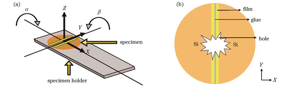
    Fig. 1. Schematic diagrams of TEM cross-section sample tilting. (a) Schematic diagram of double tilting holder; (b) orientation diagram of thin film TEM cross-section sample placed in the sample holder
    TEM results of the 40-period Mo/Si multilayer film under different crystal zone axes of the substrate Si after tilting in the α direction. (a) TEM images; (b) HRTEM images
    Fig. 2. TEM results of the 40-period Mo/Si multilayer film under different crystal zone axes of the substrate Si after tilting in the α direction. (a) TEM images; (b) HRTEM images
    Crystallography of [100] single-crystal Si wafer substrate[19]
    Fig. 3. Crystallography of [100] single-crystal Si wafer substrate19
    Schematic diagrams of TEM sample tilting in the α direction. (a) XZ plan; (b) YZ plan
    Fig. 4. Schematic diagrams of TEM sample tilting in the α direction. (a) XZ plan; (b) YZ plan
    TEM images of the 40-period Mo/Si multilayer film under different crystal zone axes of the substrate Si after tilting in the β direction
    Fig. 5. TEM images of the 40-period Mo/Si multilayer film under different crystal zone axes of the substrate Si after tilting in the β direction
    Thickness change of the 40-period Mo/Si multilayer film after tilting in the β direction
    Fig. 6. Thickness change of the 40-period Mo/Si multilayer film after tilting in the β direction
    Schematic diagram of TEM sample tilting in the β direction
    Fig. 7. Schematic diagram of TEM sample tilting in the β direction
    Calculation results of relative error δ varies with the tilting angle β. (a) Thin films with Z=50 nm and different t0; (b) thin films with t0=5 nm and different Z
    Fig. 8. Calculation results of relative error δ varies with the tilting angle β. (a) Thin films with Z=50 nm and different t0; (b) thin films with t0=5 nm and different Z
    Crystal orientationTilt(αβTotal thickness /nmD /nmdMo /nmdSi /nm
    Non-tilt(0,0)356.87.0434.0963.056
    [110](-4.33°,-1.57°)355.77.0474.0542.983
    [210](13.99°,-2.47°)356.47.0163.9673.038
    [310](22.27°,-3.15°)356.67.0533.9893.063
    [100](40.44°,-4.94°)357.07.0534.0822.943
    Table 1. Thickness change of the 40-period Mo/Si multilayer film after tilting in the α direction
    Crystal orientationTilt(αβ

    Total

    thickness /nm

    Non-tilt(0,0)356.8
    [332](-1.75°,-21.67°)355.6
    [111](-0.06°,-29.81°)346.8
    Table 2. Thickness change of the 40-period Mo/Si multilayer film after tilting in the β direction
    Ge Zhang, Yun Cui, Jiaoling Zhao, Tao Wang, Yuan'an Zhao. Effect of Sample Tilting Angle on the Characterization of Nanofilms by Transmission Electron Microscopy[J]. Acta Optica Sinica, 2024, 44(2): 0231001
    Download Citation