• Photonics Research
  • Vol. 8, Issue 12, 1888 (2020)
Wei Luo1、2、†, Ying Xue1、†, Jie Huang1, Liying Lin1, Bei Shi1, and Kei May Lau1、*
Author Affiliations
  • 1Department of Electronic and Computer Engineering, The Hong Kong University of Science and Technology, Clear Water Bay, Kowloon, Hong Kong, China
  • 2e-mail: wluoag@connect.ust.hk
  • show less
    DOI: 10.1364/PRJ.403938 Cite this Article Set citation alerts
    Wei Luo, Ying Xue, Jie Huang, Liying Lin, Bei Shi, Kei May Lau. Comparison of growth structures for continuous-wave electrically pumped 1.55 μm quantum dash lasers grown on (001) Si[J]. Photonics Research, 2020, 8(12): 1888 Copy Citation Text show less
    (a) AFM image of 1.1 μm GaAs on planar silicon after TCA, and RMS of the 10 μm×10 μm area is 1.1 nm. (b) AFM image of 3.1 μm InP on GoPS, and RMS of the 10 μm×10 μm area is 2.8 nm. (c) Representative plan view TEM image of InP on GoPS.
    Fig. 1. (a) AFM image of 1.1 μm GaAs on planar silicon after TCA, and RMS of the 10  μm×10  μm area is 1.1 nm. (b) AFM image of 3.1 μm InP on GoPS, and RMS of the 10  μm×10  μm area is 2.8 nm. (c) Representative plan view TEM image of InP on GoPS.
    Schematic diagram of QDashes grown on InP/GoPS with different structures. (a) Sample A: Al composition of InAlGaAs is changed from 0.29 to 0.24. (b) Sample B: low temperature cap layer is changed from InAlGaAs to InGaAs based on Sample A. (c) Sample C: Al composition of InAlGaAs is changed back to 0.29, and the thickness of InAlGaAs is increased from 200 nm to 300 nm based on Sample B.
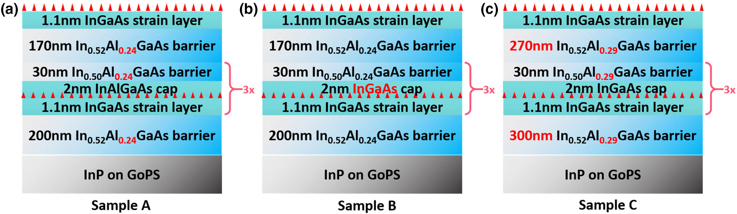
    Fig. 2. Schematic diagram of QDashes grown on InP/GoPS with different structures. (a) Sample A: Al composition of InAlGaAs is changed from 0.29 to 0.24. (b) Sample B: low temperature cap layer is changed from InAlGaAs to InGaAs based on Sample A. (c) Sample C: Al composition of InAlGaAs is changed back to 0.29, and the thickness of InAlGaAs is increased from 200 nm to 300 nm based on Sample B.
    (a) Cross-section TEM image of InP/GoPS template. (b) 1 μm×1 μm AFM image of top exposed QDashes grown on InP/GoPS (Sample B). (c) Cross-section TEM image of QDashes grown on InP/GoPS with zoomed-in image as inset. (d) Room temperature PL of three-layer QDashes grown on Samples A, B, and C. The measurement was cutoff at 1600 nm due to the photodetector.
    Fig. 3. (a) Cross-section TEM image of InP/GoPS template. (b) 1  μm×1  μm AFM image of top exposed QDashes grown on InP/GoPS (Sample B). (c) Cross-section TEM image of QDashes grown on InP/GoPS with zoomed-in image as inset. (d) Room temperature PL of three-layer QDashes grown on Samples A, B, and C. The measurement was cutoff at 1600 nm due to the photodetector.
    (a) Schematic diagram (not to scale) and (b) 70° tilted cross-section SEM image of a fabricated Fabry–Perot (FP) laser on InP/GoPS.
    Fig. 4. (a) Schematic diagram (not to scale) and (b) 70° tilted cross-section SEM image of a fabricated Fabry–Perot (FP) laser on InP/GoPS.
    (a) Representative I–V curves of fabricated devices with turn-on voltage of around 0.7 V. (b) Room temperature pulsed lasing L-I curves of different size FP lasers on Sample A. (c) Room temperature continuous-wave lasing L-I curves of different size FP lasers on Samples B and C. (d) Pulsed lasing threshold currents of 6 μm×1 mm lasers on Samples A, B, and C at different temperatures.
    Fig. 5. (a) Representative I–V curves of fabricated devices with turn-on voltage of around 0.7 V. (b) Room temperature pulsed lasing L-I curves of different size FP lasers on Sample A. (c) Room temperature continuous-wave lasing L-I curves of different size FP lasers on Samples B and C. (d) Pulsed lasing threshold currents of 6  μm×1  mm lasers on Samples A, B, and C at different temperatures.
    (a) L-I curve of an 8 μm×1.5 mm deep-etched FP laser on Sample B with the lowest threshold current density of 1.5 kA/cm2 under CW lasing at room temperature. Inset is the L-I curve plotted in logarithmic scale. (b) Room temperature CW lasing spectrum of a deep-etched FP laser on Sample B.
    Fig. 6. (a) L-I curve of an 8  μm×1.5  mm deep-etched FP laser on Sample B with the lowest threshold current density of 1.5  kA/cm2 under CW lasing at room temperature. Inset is the L-I curve plotted in logarithmic scale. (b) Room temperature CW lasing spectrum of a deep-etched FP laser on Sample B.
    Wei Luo, Ying Xue, Jie Huang, Liying Lin, Bei Shi, Kei May Lau. Comparison of growth structures for continuous-wave electrically pumped 1.55 μm quantum dash lasers grown on (001) Si[J]. Photonics Research, 2020, 8(12): 1888
    Download Citation