Author Affiliations
1College of Science, MIIT Key Laboratory of Aerospace Information Materials and Physics, Key Laboratory for Intelligent Nano Materials and Devices, Nanjing University of Aeronautics and Astronautics, Nanjing 211106, China2e-mail: cxkan@nuaa.edu.cnshow less
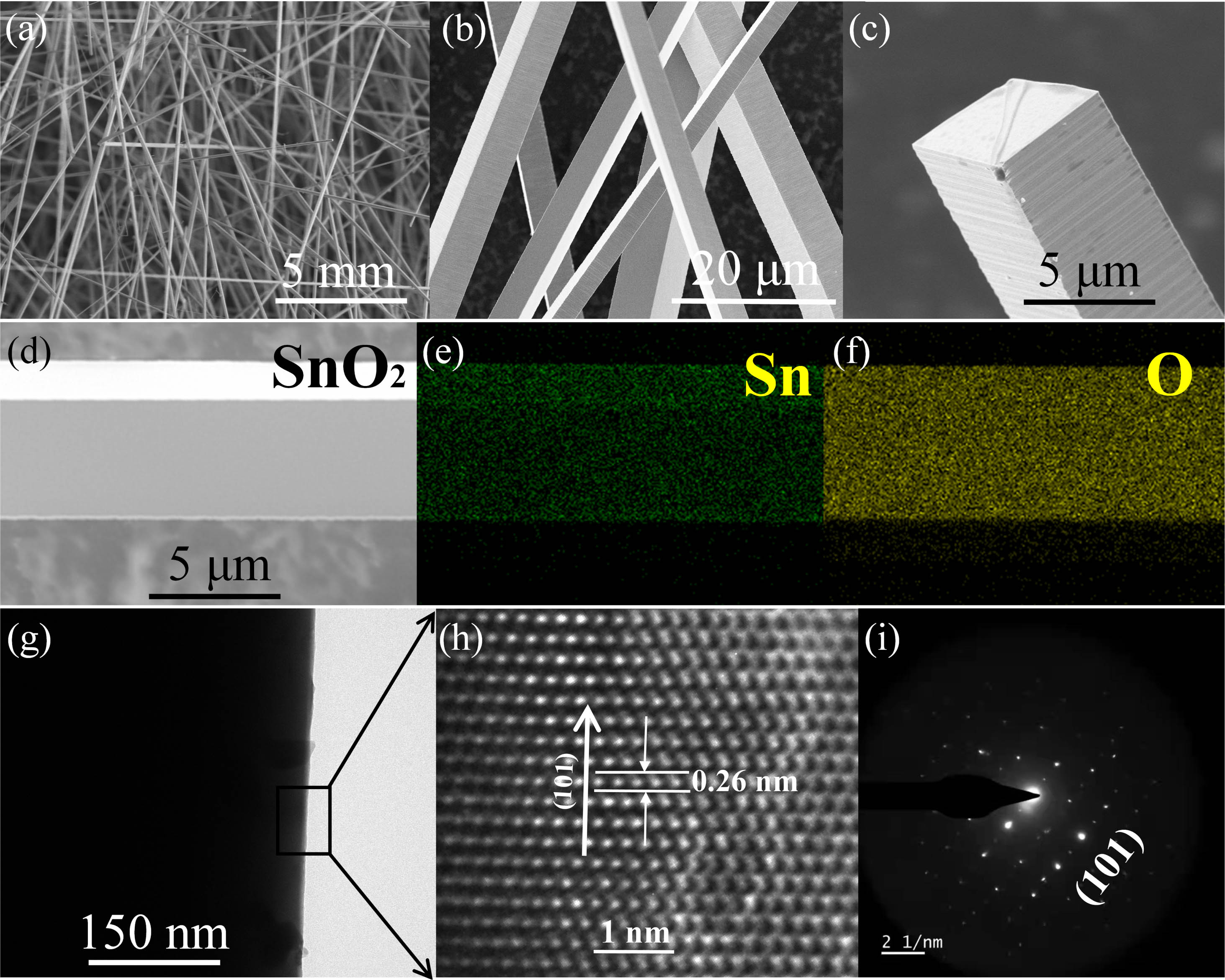
Fig. 1. Characterization of the prepared SnO2 MWs. (a) Optical photograph of individual SnO2 MWs. (b) Enlarged SEM image of several SnO2 MWs. (c) Quadrilateral cross section of an individual SnO2 MW. (d)–(f) EDS elemental mapping results of Sn and O species from a selected MW. (g) Lower-resolution TEM picture of a single SnO2 wire, the diameter was measured to about 500 nm. (h) Corresponding high-resolution TEM image marked in (g). (i) SAED image of a SnO2 wire. It suggests that the as-grown SnO2 wires are preferentially exposing (101) orientation.
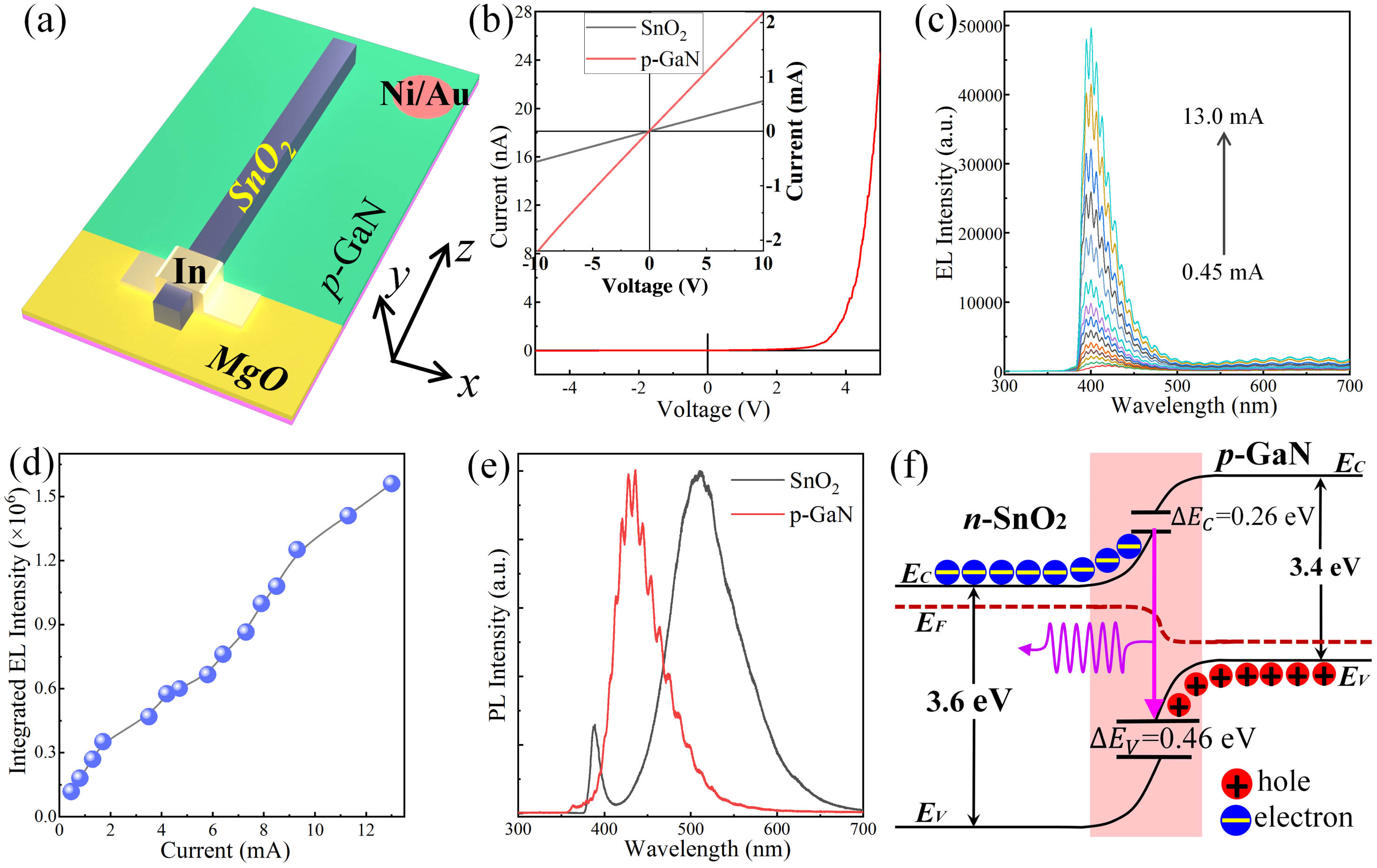
Fig. 2. Characterization of the fabricated n-SnO2 MW/p-GaN heterojunction LED. (a) Straightforward illustration of a near-ultraviolet LED structure, which is made of an individual SnO2 MW and p-GaN substrate. In the device architecture, In and Ni/Au are employed as electrodes for the current injection. (b) I-V curve of the fabricated SnO2 MW/p-GaN heterostructure, suggesting diode-like rectifying characteristic. Inset: I-V curves of an individual SnO2 MW and p-type GaN template, yielding ohmic contact behaviors. (c) The EL spectra as a function of the input current varied from 0.45 to 13.0 mA. (d) Variation of integrated EL intensity versus injection current. (e) Normalized PL spectra of a SnO2 MW and p-type GaN substrate, respectively. (f) Schematic of the energy band diagram of n-SnO2 MW/p-GaN heterojunction.
Fig. 3. When illuminated electrically at forward biasing condition, optical microscopic EL pictures of the as-fabricated n-SnO2 MW/p-GaN LED were captured using a CCD, with the input current varied in the range of 3.0–13.0 mA. The scale bar is 25 μm.
Fig. 4. Characterization of ultraviolet photodetecting features of the prepared n-SnO2 MW/p-GaN heterojunction device. (a) Schematic diagram of the n-SnO2 MW/p-GaN heterojunction photodetecting device. (b) The comparison of photocurrent on the fabricated n-SnO2 MW/p-GaN heterojunction device under 360 nm light (upper, red) and dark (lower, blue). (c) I-V curves of the fabricated n-SnO2 MW/p-GaN heterojunction photodetection apparatus under the dark, and illumination at different wavelengths in the ultraviolet regions. (d) Contour plot of the responsivity R of the as-prepared n-SnO2 MW/p-GaN heterojunction photodetection apparatus as a function of light wavelengths of the ultraviolet illumination, and different bias. (e) The detectivity of as-fabricated n-SnO2 MW/p-GaN heterojunction photodetection device as a function of wavelength at −3.0 V bias. (f) By varying the applied bias voltage in the region of −5.0 to −1.0 V, comparison of LDR spectra of as-prepared photodetectors when operated at different incident wavelengths.
Fig. 5. (a) Light power-dependent photoresponse under ultraviolet illumination at the time scale. The device was illuminated at the light wavelength of 360 nm, and measured at a reverse bias of −3.0 V. Inset: the enlarged portions of I-t curve of the device from the highlighted part in (a), which operated upon the ultraviolet light illumination at the wavelength of 360 nm. (b) Logarithmic plot of the photocurrent versus incident light irradiation power at a reverse bias of −3.0 V. (c) Responsivity and (d) detectivity of the as-constructed n-SnO2 MW/p-GaN heterojunction photodetector in terms of light intensity at −3 V bias.
Fig. 6. (a) I-t curve of the fabricated n-SnO2 MW/p-GaN heterojunction photodetector under 265 switching cycles of ultraviolet light illumination. (b) The variations of photocurrent and dark current when the photodetector was stored in the lab in ambient air for different time (∼70 days). (c) Rise time and decay time of the n-SnO2 MW/p-GaN heterojunction photodetector measured at the bias of −3 V. (d) Energy band diagram of the photodetector operated upon ultraviolet light irradiation. Under ultraviolet illumination, the generated electrons transport toward n-type SnO2 MW on the conduction band, while the holes transport toward p-type GaN layer on the valence band.
Photodetector | Wavelength | Responsivity | Detectivity [Jones] | EQE | UV/vis Ratio | Response Time | Refs. |
---|
nanowire | 320 nm | – | – | % | – | – | [12] | film | 290 nm | 23 mA/W | – | 10% | 200 | 128/91 ms | [60] | microrod | 260 nm | | – | | | | [41] | nanonets | 320 nm | – | – | – | – | | [35] | nanowire arrays | 370 nm | 0.36 mA/W | | – | 1.8 | 0.72/1.78 s | [61] | nanofibers | 300 nm | – | – | – | – | 32.2/7.8 s | [37] | MW/PEDOT:PSS | 450 nm | 0.018 mA/W | – | – | – | | [18] | core-shell | 300 nm | 1.6 mA/W | | 0.63% | 500 | 0.045/1.17 ms | [29] | | 360 nm | 185 mA/W | | 74% | | 310 ns/61 μs | [2] | | 320 nm | 1900 mA/W (3 V) | | – | – | 0.03/1.94 ms (0 V) | [30] | MW/GaN | 360 nm | 1450 mA/W | | 497% | | 9.2/51 ms | This work |
|
Table 1. Comparison between the Fabricated n-SnO2 MW/p-GaN Heterojunction Photodetector in This Work and Other Previously Reported Works