• Photonics Research
  • Vol. 9, Issue 12, 2475 (2021)
Tong Xu1, Mingming Jiang1、*, Peng Wan1, Kai Tang1, Daning Shi1, and Caixia Kan1、2
Author Affiliations
  • 1College of Science, MIIT Key Laboratory of Aerospace Information Materials and Physics, Key Laboratory for Intelligent Nano Materials and Devices, Nanjing University of Aeronautics and Astronautics, Nanjing 211106, China
  • 2e-mail: cxkan@nuaa.edu.cn
  • show less
    DOI: 10.1364/PRJ.441999 Cite this Article Set citation alerts
    Tong Xu, Mingming Jiang, Peng Wan, Kai Tang, Daning Shi, Caixia Kan. Bifunctional ultraviolet light-emitting/detecting device based on a SnO2 microwire/p-GaN heterojunction[J]. Photonics Research, 2021, 9(12): 2475 Copy Citation Text show less

    Abstract

    SnO2 has attracted considerable attention due to its wide bandgap, large exciton binding energy, and outstanding electrical and optoelectronic features. Owing to the lack of reliable and reproducible p-type SnO2, many challenges on developing SnO2-based optoelectronic devices and their practical applications still remain. Herein, single-crystal SnO2 microwires (MWs) are acquired via the self-catalyzed approach. As a strategic alternative, n-SnO2 MW/p-GaN heterojunction was constructed, which exhibited selectable dual-functionalities of light-emitting and photodetection when operated by applying an appropriate voltage. The device illustrated a distinct near-ultraviolet light-emission peaking at 395.0 nm and a linewidth 50 nm. Significantly, the device characteristics, in terms of the main peak positions and linewidth, are nearly invariant as functions of various injection current, suggesting that quantum-confined Stark effect is essentially absent. Meanwhile, the identical n-SnO2 MW/p-GaN heterojunction can also achieve photovoltaic-type light detection. The device can steadily feature ultraviolet photodetecting ability, including the ultraviolet/visible rejection ratio (R360 nm/R400 nm) 1.5×10³, high photodark current ratio of 105, fast response speed of 9.2/51 ms, maximum responsivity of 1.5 A/W, and detectivity of 1.3×10¹³ Jones under 360 nm light at -3 V bias. Therefore, the bifunctional device not only displays distinct near-ultraviolet light emission, but also has the ability of high-sensitive ultraviolet photodetection. The novel design of n-SnO2 MW/p-GaN heterojunction bifunctional systems is expected to open doors to practical application of SnO2 microstructures/nanostructures for large-scale device miniaturization, integration and multifunction in next-generation high-performance photoelectronic devices.

    1. INTRODUCTION

    Fabrication of multifunctional optoelectronic devices, especially for the low-dimensional devices, has regarded as the rising demand of energy conservation, miniaturization, high-integration, being portable in many daily life aspects [18]. Because of its wide bandgap and a high exciton-binding energy (3.62  eV, 130  meV at room temperature), high quantum efficiency, stability and high electron mobility, tin dioxide (SnO2) is frequently used as a potential candidate to develop many practical devices, such as gas sensors, transparent conductors, photodetectors, light-emitting devices, and solar cells [915]. Owing to its natural n-type conductivity, it is still a serious bottleneck to prepare stable and reproducible p-type SnO2. Alternatively, the p-GaN film layer has been commonly utilized to fabricate SnO2-based heterojunction optoelectronic devices, due to the wide application and mature doping technology [2,14,1618]. Nevertheless, being restricted to the dipole-forbidden and intrinsic defects including Sn interstitials, dangling bonds, or oxygen vacancies, the vast majority of the previously reported works have illustrated that bulk SnO2-based emission devices mostly emit broad luminescence at the visible wavelengths, instead of ultraviolet light emission [15,19]. Lately, low dielectric layers, such as MgO and AlN, have been introduced into SnO2/GaN-based heterojunction LEDs to improve the device performance. In addition, low-dimensional SnO2, including quantum dots, nanowire, nanotubes, nanowire arrays, microwire/rods, and so on, has been prepared to construct ultraviolet light sources, and eventually used to break through the dilemma of the “forbidden” bandgap due to large surface-to-volume ratios, low cost, strong radiation hardness, and high chemical stability [14,16,17,20].

    As a typical wide-bandgap semiconductor, SnO2 has attracted great attention in the field of fabricating ultraviolet photodetection devices [8,2126]. Based on the photoelectric effect, SnO2-based structures and devices can transform optical information into electrical signals, providing a competitive candidate to develop ultraviolet photodetecting devices. Numerous studies reported that SnO2 thin film, nanowire, nanonet, nanofiber, nanobelt, and microrod/wires have been utilized to fabricate ultraviolet photodetectors with their applications in missile early warning, flame sensing, environmental monitoring, and wireless communications [2,2731]. Many groups have presented that SnO2 nanowires have been extensively used to construct high-performance ultraviolet photodetectors [12,13,3234]. For instance, Chen et al. fabricated SnO2NiO heterojunction nanonets, exhibiting a high ultraviolet detectivity [35]; and Tian et al. reported ZnOSnO2 heterojunction nanofibers, yielding a high photocurrent in ultraviolet region [32,3638]. However, the device performances, including the dark current and response time of the works mentioned above, are still dissatisfactory [18,39,40]. There remains a lot of work to do to improve the response time and photocurrent while reducing the dark current of the as-constructed SnO2-based photodetecting devices [31,4146].

    To satisfy some special requirements in practical applications with regard to excellent electroluminescent and photovoltaic properties, studies on the synthesis of low-dimensional semiconductors and the construction of optoelectronic devices with bifunctional electronics are particularly important [5,4750]. In this work, individual SnO2 microwires (MWs) with high crystallinity and well-defined geometries have been prepared utilizing a facile vapor transport deposition (CVD) method. Employing p-type GaN as the hole transporting layer, we demonstrate an ultraviolet light emission and detection dual-functioning device based on a single SnO2 MW upon the operation of both forward and reverse biasing conditions, respectively. As the forward bias beyond the turn-on voltage, the fabricated n-SnO2 MW/p-GaN heterojunction device exhibits significant near-ultraviolet electroluminescence (EL) with a pronounced peak luminescence at 395.0 nm, and the spectral linewidth is extracted to about 50 nm. Simultaneously, the heterojunction also demonstrates excellent ultraviolet photodetecting features, containing a large responsivity of 1.5 A/W, a detectivity of 1.3×10¹³ Jones, a high external quantum efficiency (EQE) of 497%, a large photo-to-dark current (Ion/Ioff) ratio of 105, an ultraviolet/visible rejection ratio of about 1.5×10³, and a fast response speed of 9.2/51 ms under 360 nm light at a reverse bias of 3.0  V. These experimental results exhibit that the simple and easy fabrication of n-SnO2 MW/p-GaN heterojunction provides a new and promising scheme for developing ultraviolet bifunctional optoelectronic devices, as well as for practical applications.

    2. EXPERIMENTAL SECTION

    A. Synthesis of Individual SnO2 MWs

    Single-crystal SnO2 MWs were prepared utilizing a simple CVD method [24,29,30]. In the process of preparing microstructured SnO2, a high-temperature tube furnace is used as the crystal growth equipment. A mixture of high-purity powders of SnO2 and graphite (C) (the weight ratio of 1:1) was put in a corundum boat. A cleaned Si wafer was placed on a corundum boat to collect the samples. The growth procedure was summarized as follows: (1) to guarantee that tube furnace was an oxygen-deficient environment, a constant flow of argon (Ar) (99.99%) (125 sccm) was first introduced into the tube furnace; (2) the corundum boat was put into a quartz tube, and the precursor mixture was placed at the hottest zone; (3) the temperature was raised to 1100°C at a rate of 20°C per minute, and served as growth temperature; (4) with the oxygen-deficient composited condition maintained for 1h, 10% oxygen (O2) was introduced into the furnace chamber as the growth gas for about 30 min; (5) the furnace chamber was then naturally cooled to room temperature. SnO2 product can be collected around the Si wafer. The diameter of the wires varies in the region of 0.5–20 μm, and their length can reach up to 1 cm. By optimizing the growth condition including the growth temperature, and the carrier gas, SnO2 MWs with higher crystallization quality can be improved.

    B. Fabrication of n-SnO2 MW/p-GaN Heterojunction

    A heterostructured device made of an individual n-SnO2 MW and p-type GaN substrate was prepared. In the heterostructure, commercially purchased p-type GaN substrate was utilized as the hole transporting layer. The device preparation is summarized as follows: (1) Ni/Au films with the thickness of 30/40 nm were first prepared on an activated p-type GaN layer; (2) MgO insulating films (100  nm in thickness) were deposited on one side of the GaN film utilizing electron beam heating evaporation; (3) a single SnO2 MW with the diameter of about 10 μm was subsequently placed across the p-GaN film and MgO layer, and an In particle was fixed on the wire on the MgO layer; thus, the MgO layer serving as an insulating layer was utilized to prevent the direct contacting between the In electrode and the p-GaN substrate. In the device structure, In and Ni/Au were employed as electrodes for the current injection. The device configuration is schematically depicted later in the paper [51,52].

    3. RESULTS AND DISCUSSION

    A. n-SnO2 MW/p-GaN Heterojunction LED

    As we described in the experimental section, individual SnO2 MWs with well-defined geometries, specifically for the quadrilateral cross section, were successfully prepared [24,29,30]. The optical picture of as-grown MWs is shown in Fig. 1(a). A scanning electron microscopy (SEM) image of SnO2 MWs is displayed in Fig. 1(b). It illustrates that the average diameter of the as-synthesized MWs is approximately about 5 μm. In addition, a quadrilateral cross section can also be observed in Fig. 1(c). The elemental mapping of an individual SnO2 MW was determined by energy-dispersive X-ray spectroscopy (EDS). As shown in Figs. 1(d)–1(f), the elements of Sn and O are uniformly distributed throughout a single wire. Typical transmission electron microscopy (TEM) images of an individual SnO2 wire (the diameter 500  nm) with a straight boundary were examined, and its high-resolution TEM picture is displayed in Fig. 1(g). From the figure, the wire demonstrates clear lattice fringes, and the interplanar space is extracted to be about 0.260 nm [30,31]. Further, the single-crystalline character of the as-synthesized SnO2 wire was featured by using the electron diffraction (SAED) pattern, which corresponded to the (101) plane of rutile SnO2 [see Fig. 1(i)]. Therefore, the as-synthesized SnO2 MWs were well-crystallized in the single-crystal rutile structure [35,41].

    Characterization of the prepared SnO2 MWs. (a) Optical photograph of individual SnO2 MWs. (b) Enlarged SEM image of several SnO2 MWs. (c) Quadrilateral cross section of an individual SnO2 MW. (d)–(f) EDS elemental mapping results of Sn and O species from a selected MW. (g) Lower-resolution TEM picture of a single SnO2 wire, the diameter was measured to about 500 nm. (h) Corresponding high-resolution TEM image marked in (g). (i) SAED image of a SnO2 wire. It suggests that the as-grown SnO2 wires are preferentially exposing (101) orientation.

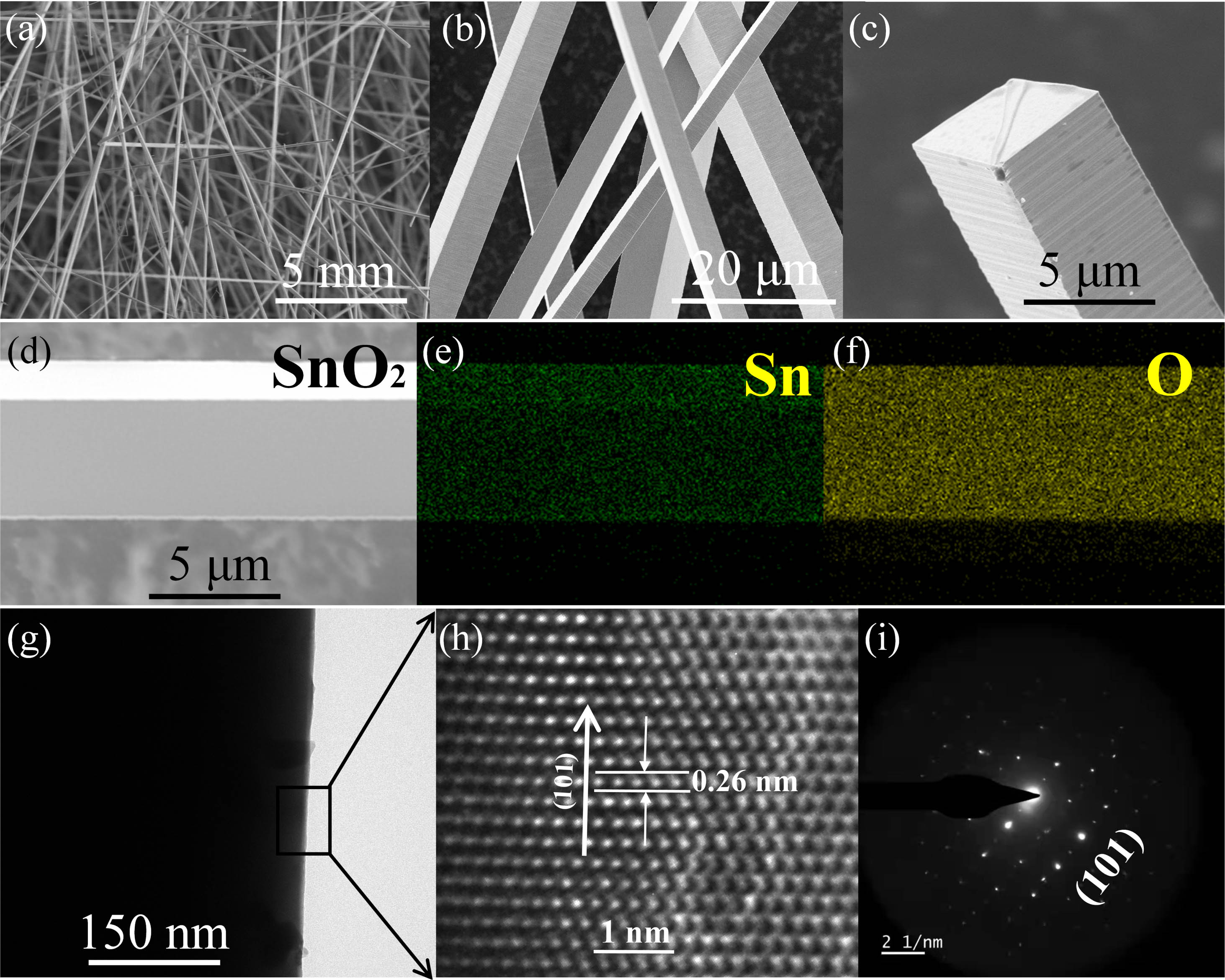
    Figure 1.Characterization of the prepared SnO2 MWs. (a) Optical photograph of individual SnO2 MWs. (b) Enlarged SEM image of several SnO2 MWs. (c) Quadrilateral cross section of an individual SnO2 MW. (d)–(f) EDS elemental mapping results of Sn and O species from a selected MW. (g) Lower-resolution TEM picture of a single SnO2 wire, the diameter was measured to about 500 nm. (h) Corresponding high-resolution TEM image marked in (g). (i) SAED image of a SnO2 wire. It suggests that the as-grown SnO2 wires are preferentially exposing (101) orientation.

    Characterization of the fabricated n-SnO2 MW/p-GaN heterojunction LED. (a) Straightforward illustration of a near-ultraviolet LED structure, which is made of an individual SnO2 MW and p-GaN substrate. In the device architecture, In and Ni/Au are employed as electrodes for the current injection. (b) I-V curve of the fabricated SnO2 MW/p-GaN heterostructure, suggesting diode-like rectifying characteristic. Inset: I-V curves of an individual SnO2 MW and p-type GaN template, yielding ohmic contact behaviors. (c) The EL spectra as a function of the input current varied from 0.45 to 13.0 mA. (d) Variation of integrated EL intensity versus injection current. (e) Normalized PL spectra of a SnO2 MW and p-type GaN substrate, respectively. (f) Schematic of the energy band diagram of n-SnO2 MW/p-GaN heterojunction.

    Figure 2.Characterization of the fabricated n-SnO2 MW/p-GaN heterojunction LED. (a) Straightforward illustration of a near-ultraviolet LED structure, which is made of an individual SnO2 MW and p-GaN substrate. In the device architecture, In and Ni/Au are employed as electrodes for the current injection. (b) I-V curve of the fabricated SnO2 MW/p-GaN heterostructure, suggesting diode-like rectifying characteristic. Inset: I-V curves of an individual SnO2 MW and p-type GaN template, yielding ohmic contact behaviors. (c) The EL spectra as a function of the input current varied from 0.45 to 13.0 mA. (d) Variation of integrated EL intensity versus injection current. (e) Normalized PL spectra of a SnO2 MW and p-type GaN substrate, respectively. (f) Schematic of the energy band diagram of n-SnO2 MW/p-GaN heterojunction.

    The illustration in Fig. 2(a) is a schematic of a heterojunction LED, which is made of a SnO2 MW and p-type GaN substrate. In the device configuration, the p-type GaN substrate serves as the hole transporting layer [2,14]. To study the device performance, the electrical contacting character of the n-SnO2 MW/p-GaN heterojunction was first measured by using a Keysight semiconductor device analyzer (B1500A). The current-voltage (I-V) curve is plotted in Fig. 2(b), indicating that the curve illustrates a well-defined diode-like rectifying behavior. To investigate the electrical behavior, the electronic transport properties of an individual SnO2 MW were examined, and the I-V curve is illustrated in the inset of Fig. 2(b) (in the electrical measurement, In particles serve as the electrodes). The plotted curve illustrates linear behavior, confirming that the In electrode makes a good ohmic contact with the SnO2 MW. Ni/Au was evaporated on the p-GaN template utilizing the electron-beam evaporation system. Afterwards, an annealing treatment was further implemented in air. An I-V curve shown in the inset of Fig. 2(b) displays a linear feature, and thus, ohmic contact behavior was formed between the Ni/Au and p-GaN substrate (the red solid line) [7,53]. The diode-like rectification characteristic is attributed to the high-quality heterojunction formed between the n-SnO2 MW and p-GaN substrate. Specifically, the device has a turn-on voltage of 4.0V, and a negligibly small leakage current, which was evaluated to 3.9×10¹¹  A even at 5  V bias. Therefore, an n-SnO2 MW/p-GaN heterojunction can be utilized to construct a one-dimensional wired optoelectronic device.

    Varying the forward bias above the turn-on voltage, the electrically driven luminescence from the as-fabricated n-SnO2 MW/p-GaN heterojunction LED was tested by utilizing the PIXIS 1024BR CCD detection system at room temperature. Figure 2(c) displays the collected EL spectra. It represents a dominant near-ultraviolet emission with a main peak wavelength of about 395.0 nm. Noticeably, the main peak wavelengths keep an almost constant value by increasing the injection current, while the spectral linewidths of the EL spectra are checked to about 50 nm, and the linewidths are nearly invariant with various input currents. Compared with conventional GaN-based ultraviolet light emitters which severely suffer from quantum-confined Stark effect, the fabricated n-SnO2 MW/p-GaN heterojunction LEDs exhibit extraordinary stability. Figure 2(d) plots the driving current-dependent integrated EL intensity, showing nearly linear characteristics. The linear rise of integrated EL intensity with regard to the input current indicates a very small Shockley–Read–Hall recombination coefficient in the SnO2 MW LED. Therefore, the well-formed one-dimensional wired n-SnO2/p-GaN heterojunction can be ascribed to the dramatically lower defects and negligible nonradiative recombination at the surfaces of SnO2 nanostructures/microstructures [2,16,17].

    To exploit the near-ultraviolet EL features of the as-fabricated n-SnO2 MW/p-GaN heterojunction LED, optical characterization of a SnO2 MW and GaN template was performed by using He–Cd laser at an excitation wavelength of 325 nm. The photoluminescence (PL) spectra were collected by utilizing a spectrometer via an Andor Newton electron multiplying CCD camera (Horiba Jobin-Yvon iHR500). The PL spectrum of a SnO2 MW illustration in Fig. 2(e) (the black solid line) demonstrates that ultraviolet emission peaking at 380.0 nm was obtained, accompanied with a much stronger broadband emission in the visible band (the peak position locates at 510 nm). By optimizing the CVD method, the near-band-edge related PL can be acquired in the ultraviolet region due to the breakthrough of dipole forbidden rule. The broader and stronger light emission in the visible region is assigned to the radiative recombination, which is connected with the deep-level defects. It suggests that the as-grown SnO2 MWs possess relative high crystal quality [2,14]. The optical characterization of the p-type GaN substrate was also performed by utilizing a He–Cd laser as an excitation laser source. Figure 2(e) displays the PL spectrum (the red solid line), illustrating that the main PL wavelength positions at around 435.5 nm, and the spectral linewidth is measured to be 50 nm. Accordingly, the EL peak energy of the device cannot be matched well with the near-band energy, or the deep-level energy of the SnO2 MW; meanwhile, the near-ultraviolet EL cannot be matched with light radiation from direct band-to-band transition of the GaN film. Therefore, the EL results could be attributed to the radiative recombination at the n-SnO2/p-GaN interface [2,14,17].

    Compared with PL results of the SnO2 MW and GaN layer, it is concluded that the near-ultraviolet EL of the fabricated LED cannot be simply derived from either the SnO2 MW or the p-GaN substrate. The origin of the near-ultraviolet EL was examined. According to the electron affinities of SnO2 (4.50  eV) and GaN (4.20  eV), a Type II energy band structure can be created at the n-SnO2/p-GaN heterostructure, as depicted in Fig. 2(f) [2,30,45]. As the hole concentration in the p-type GaN template 1017 is much approximate to the electron concentration in the n-SnO2 MW, thus, a formation of wider depletion region in the SnO2 MW could be yielded. It is inferred that a conduction-band offset of ΔEc is evaluated to be 0.26 eV, while the valence band offset of ΔEv is evaluated to about 0.46 eV, producing a band discontinuity at the SnO2/GaN interface. Owing to the much smaller band offset (ΔEc0.26  eV, ΔEv0.46  eV), electrons in the SnO2 MW can leak into the p-type GaN layer, while the injected holes into the fabricated heterojunction device can leak from the p-type GaN layer into the n-SnO2 MW. The obtained EL may be composed of the light emitting from the SnO2 MW, GaN layer, and the SnO2/GaN interface. In particular, the ΔEv is considerably larger than ΔEc, and it can be figured out that electron injection from the n-SnO2 MW into the p-GaN layer is much more advantageous by comparing with the hole injection. Consequently, efficient radiative recombinations of carriers are principally happening at the SnO2/GaN interface, explaining the origin of near-ultraviolet EL upon the electrical excitation [2,14,17].

    The near-ultraviolet emission characteristics of one-dimensional wired LED were studied by using a high numerical aperture microscope objective via a CCD camera (Olympus). Varying the injection current in the range of 3.0–13.0 mA, the optical microscopic EL images of blue–violet illuminating were captured, as shown in Fig. 3. From the figure, the near-ultraviolet light is mainly emitted out along both the lateral edges of the quadrilateral MW, and the EL intensity is periodically distributed around the quadrilateral microresonator. For the first time, the n-SnO2 MW/p-GaN heterojunction emitting at 395.0  nm is designed. The success of an individual SnO2 MW with good crystal quality in designing ultraviolet LEDs paves the way toward practical applications of SnO2 microstructure/nanostructure-based light sources. In addition, several light-emission devices on account of the n-SnO2 MW/p-GaN heterojunction architecture were also constructed, as we described in Section 2. It is evidenced that the one-dimensional wired n-SnO2/p-GaN heterojunction can be utilized to construct low-dimensional near-ultraviolet light sources. The fabricated LEDs demonstrated excellent stability and reproducibility, which are understandable due to the outstanding durability of well-crystallized SnO2 MWs.

    When illuminated electrically at forward biasing condition, optical microscopic EL pictures of the as-fabricated n-SnO2 MW/p-GaN LED were captured using a CCD, with the input current varied in the range of 3.0–13.0 mA. The scale bar is 25 μm.

    Figure 3.When illuminated electrically at forward biasing condition, optical microscopic EL pictures of the as-fabricated n-SnO2 MW/p-GaN LED were captured using a CCD, with the input current varied in the range of 3.0–13.0 mA. The scale bar is 25 μm.

    B. n-SnO2 MW/p-GaN Heterojunction Photodetector

    As we described above, the fabricated n-SnO2 MW/p-GaN heterojunction also shows good LED-like characteristics with a negligible leakage current. Due to the much lower dark current, the n-SnO2 MW/p-GaN heterojunction for fabricating high-performance photodetectors, which work at the ultraviolet wavelengths, was further examined. To this regard, the n-SnO2 MW/p-GaN heterojunction feature as an ultraviolet photodetector was successfully demonstrated. A typical device configuration is shown in Fig. 4(a). In the device configuration, Ni/Au film deposited on the p-GaN film is employed as the cathode; while the In particle fixed on one end of the MW serves as the anode [2,29,30,54]. The electrical properties of the prepared photodetector under dark and ultraviolet radiation were tested at room temperature. As seen in Fig. 4(b), the I-V curve measured in the dark exhibits excellent rectification characteristics [blue solid line; also see Fig. 2(b)]. At 5 V bias, the current is about 2.5×10⁸  A, while the reverse leakage current at 5  V is less than 3.9×10¹¹  A. Furthermore, the rectification ratio of the device was 6.5×10² at the biases of ±5  V. When exposed under the radiation of 360 nm light, the nonlinear I-V curve (red solid line) of the heterojunction photodetector represents an observable photoresponse. It shows an off-state current (less than 1.5×10⁶  A) at the reverse bias and an on-state current (approaching 1.9×10⁵  A) at the forward bias, suggesting a traditional p-n diode behavior.

    Characterization of ultraviolet photodetecting features of the prepared n-SnO2 MW/p-GaN heterojunction device. (a) Schematic diagram of the n-SnO2 MW/p-GaN heterojunction photodetecting device. (b) The comparison of photocurrent on the fabricated n-SnO2 MW/p-GaN heterojunction device under 360 nm light (upper, red) and dark (lower, blue). (c) I-V curves of the fabricated n-SnO2 MW/p-GaN heterojunction photodetection apparatus under the dark, and illumination at different wavelengths in the ultraviolet regions. (d) Contour plot of the responsivity R of the as-prepared n-SnO2 MW/p-GaN heterojunction photodetection apparatus as a function of light wavelengths of the ultraviolet illumination, and different bias. (e) The detectivity of as-fabricated n-SnO2 MW/p-GaN heterojunction photodetection device as a function of wavelength at −3.0 V bias. (f) By varying the applied bias voltage in the region of −5.0 to −1.0 V, comparison of LDR spectra of as-prepared photodetectors when operated at different incident wavelengths.

    Figure 4.Characterization of ultraviolet photodetecting features of the prepared n-SnO2 MW/p-GaN heterojunction device. (a) Schematic diagram of the n-SnO2 MW/p-GaN heterojunction photodetecting device. (b) The comparison of photocurrent on the fabricated n-SnO2 MW/p-GaN heterojunction device under 360 nm light (upper, red) and dark (lower, blue). (c) I-V curves of the fabricated n-SnO2 MW/p-GaN heterojunction photodetection apparatus under the dark, and illumination at different wavelengths in the ultraviolet regions. (d) Contour plot of the responsivity R of the as-prepared n-SnO2 MW/p-GaN heterojunction photodetection apparatus as a function of light wavelengths of the ultraviolet illumination, and different bias. (e) The detectivity of as-fabricated n-SnO2 MW/p-GaN heterojunction photodetection device as a function of wavelength at 3.0  V bias. (f) By varying the applied bias voltage in the region of 5.0to1.0  V, comparison of LDR spectra of as-prepared photodetectors when operated at different incident wavelengths.

    When illuminated upon different light wavelengths, typical I-V curves of the device in a logarithmic plot are illustrated in Fig. 4(c) in the dark and differently illuminated lights of 300 nm (1.4  mW/cm2), 320 nm (2.0  mW/cm2), 340 nm (2.7  mW/cm2), 360 nm (3.2  mW/cm2), 380 nm (3.6  mW/cm2), and 400 nm (4.4  mW/cm2) by using a Xe lamp as light source. Shown in the figure, the fabricated n-SnO2 MW/p-GaN photodetector displays differences in the photocurrent and dark current. It indicates that the fabricated device obtains significant ultraviolet photoelectric characters. The photocurrents of the prepared device could reach 3.4×10⁵ at 5  V bias under 360 nm illumination, which is around 105 times of magnitude higher than that of the dark current. The photocurrent was lower under the illumination of 400 nm light but still kept at 2.1×10⁹  A. The ultralow dark current and super-high photocurrent indicate that the single SnO2 MW photodetector has a high signal-to-noise ratio. When the irradiated light wavelengths increase from 300 to 360 nm, the photocurrent increases gradually, which is due to the additional carrier generated by the incident light, as well as an increase of the optical power density. When the irradiated wavelength is further increased to 380 and 400 nm, the photocurrent begins to decrease gradually because the bandgap of the active layers is larger than the incident photon energy.

    To research the light wavelength selectivity of the as-fabricated n-SnO2 MW/p-GaN photodetector, the corresponding response spectra were measured. The responsivity (R), one important performance metric of the photodetector, is first introduced. The parameter R is calculated as follows [24,55,56]: R=IPIDPS.

    In the formula, IP, ID, P, and S are the photocurrent, dark current, incident optical power, and effective irradiation area, respectively. The study of the ultraviolet photodetecting behavior in terms of the illumination wavelength and applied bias for the n-SnO2 MW/p-GaN heterojunction photodetector was implemented. We calculated their photoresponse spectra. As seen in Fig. 4(d), the photodetector shows obvious response at the ultraviolet wavelength, and the photoresponse reaches its maximum value at about 360 nm. Thus, the single MW heterojunction photodetector has a representative photoresponse spectrum at the ultraviolet wavelengths. The spectral responsivities are primarily generated due to the absorption properties of the as-grown microstructured SnO2. By calculation, the ultraviolet/visible rejection ratio (R360nm/R400nm) of the heterojunction photodetector is evaluated to be 1.5×10³, indicating a prominent ultraviolet peculiarity of the photodetector. It is deduced that, increasing the reverse voltage of the device, significantly increased R can be achieved. At 1.0  V bias, the maximum responsivity R is extracted to about 0.13 A/W. Increasing the reverse voltage to be 3.0  V, the maximum responsivity R is evaluated to 1.5 A/W. As the reverse voltage increased up to 5.0  V, the maximum responsivity R is increased up to 3.5 A/W.

    To assess the device performance of the presented n-SnO2 MW/p-GaN heterojunction photodetector, the specific detectivity (D), another significant parameter of photodetectors, which shows the photodetector ability to capture very weak signals, can be expressed by the equation [41,57,58]D=RA2eID,where R is the responsivity, A is the effective irradiation area, e is the electron charge, and Id is the dark current. Due to Eq. (2), the detectivity D of the individual SnO2 MW-based photodetector as a function of the illumination wavelength was calculated. As illustrated in Fig. 4(e), the maximum D is evaluated as high as 1.3×10¹³ Jones (1  Jones=1  cm·Hz1/2·W1) under 360 nm light. The detectivity is much higher than that of commercial Si and InGaAs photodetectors [8,24,27]. Further, the detectivity D of the fabricated n-SnO2 MW/p-GaN heterojunction photodetector is also comparable to other high-performance ultraviolet photodetection devices [2,29,30,32].

    The linear dynamic range (LDR) of the n-SnO2 MW/p-GaN heterojunction device operated at various light wavelengths of ultraviolet illumination, was described by the following formula: LDR=20  log(IP/ID).

    In the formula, ID is the dark current, and IP is the photocurrent obtained at the illumination of ultraviolet light. As shown in Fig. 4(f), the LDR is obtained to be 100  dB at 360 nm, and this value is much larger than that of commercial photodetectors (66  dB). Additionally, the superhigh LDR (over 70 dB at the wavelengths of 300–360 nm) shows that the as-constructed n-SnO2 MW/p-GaN heterojunction photodetector possesses a relatively large ratio of photocurrent to dark current, and has an extremely high signal-to-noise ratio. The results display that the fabricated n-SnO2 MW/p-GaN heterojunction photodetector has excellent ultraviolet photodetecting features [2,59].

    The photosensitivity of the n-SnO2 MW/p-GaN heterojunction device was also tested at 3  V bias. Figure 5(a) displays the I-t characteristics of the photodetector under the 360 nm light utilizing irradiance with light power intensities varied in the range of 0.063.0  mW/cm2. By varying the light intensities, photocurrent responses increased steadily for the device. When the optical density is increased from 0.06 to 3.0  mW/cm2, the photoresponse of the photodetector aggrandizes with photocurrent values of 2.86 nA at 0.06  mW/cm2, 95 nA at 0.25  mW/cm2, 230 nA at 0.60  mW/cm2, and 500 nA at 1.5  mW/cm2, and then increased to 1050 nA at 3.0  mW/cm2. This phenomenon is usually explained by the ratio between the efficiency of photogeneration and the photon flux of absorption. The nonlinear relation of the variational photocurrent with light intensity can be fitted by the positive correlation Iphpθ, and p is the irradiation intensity. The exponent θ represents the photocurrent response to the intensity of incident light. In the illustration in Fig. 5(b), θ is estimated to 0.92 under 360 nm light according to the fitted data. The slight deviation is caused by the complicated processes of carrier generation, recombination, and trapping in the n-SnO2 MW/p-GaN heterojunction photodetector.

    (a) Light power-dependent photoresponse under ultraviolet illumination at the time scale. The device was illuminated at the light wavelength of 360 nm, and measured at a reverse bias of −3.0 V. Inset: the enlarged portions of I-t curve of the device from the highlighted part in (a), which operated upon the ultraviolet light illumination at the wavelength of 360 nm. (b) Logarithmic plot of the photocurrent versus incident light irradiation power at a reverse bias of −3.0 V. (c) Responsivity and (d) detectivity of the as-constructed n-SnO2 MW/p-GaN heterojunction photodetector in terms of light intensity at −3 V bias.

    Figure 5.(a) Light power-dependent photoresponse under ultraviolet illumination at the time scale. The device was illuminated at the light wavelength of 360 nm, and measured at a reverse bias of 3.0  V. Inset: the enlarged portions of I-t curve of the device from the highlighted part in (a), which operated upon the ultraviolet light illumination at the wavelength of 360 nm. (b) Logarithmic plot of the photocurrent versus incident light irradiation power at a reverse bias of 3.0  V. (c) Responsivity and (d) detectivity of the as-constructed n-SnO2 MW/p-GaN heterojunction photodetector in terms of light intensity at 3  V bias.

    When operated under 360 nm ultraviolet illumination at 3  V bias, the responsivity (R) of the fabricated n-SnO2 MW/p-GaN heterojunction photodetector reaches up to about 1.5 A/W [see Fig. 5(c)], while the corresponding detectivity (D) is extracted up to about 1.3×10¹³ Jones by varying the light intensity [see Fig. 5(d)]. The device parameters exhibit an excellent detection capability of the as-fabricated n-SnO2 MW/p-GaN heterojunction photodetector. In addition, R and D decrease with an increase of light intensity, and these phenomena may be caused by the scattering and enhanced recombination of carriers.

    The stability of the as-constructed n-SnO2 MW/p-GaN heterojunction photodetector, one critical device parameter for their practical application, is checked. When operated at a reverse bias voltage of 3.0  V, the workable stability of the as-constructed n-SnO2 MW/p-GaN photodetector was studied by utilizing 360 nm light at a light power intensity of 3.5  mW/cm2. The switching performance via the I-t curve illustrated in Fig. 6(a) shows that the obtained photocurrent and dark current possessed negligible degradation in the whole measurement, indicating reliable light operation stability at the absence of encapsulation. In addition, the Ilight/Idark ratio is up to 104, as the dark current is measured to about 104  μA. After storing in lab in ambient air condition for about 70 days, the light current and dark current of the as-constructed photodetector were recorded at different times and are plotted in Fig. 6(b). Clearly, there is a weak fluctuation of currents, and a high Ilight/Idark ratio of nearly 104 was captured under the ultraviolet illumination via a 3.5  mW/cm2 intensity even after storing in ambient air for 70 days, suggesting that the as-fabricated n-SnO2 MW/p-GaN heterojunction photodetector exhibits quite good long-term storage stability without any encapsulation [7,25,54].

    (a) I-t curve of the fabricated n-SnO2 MW/p-GaN heterojunction photodetector under 265 switching cycles of ultraviolet light illumination. (b) The variations of photocurrent and dark current when the photodetector was stored in the lab in ambient air for different time (∼70 days). (c) Rise time and decay time of the n-SnO2 MW/p-GaN heterojunction photodetector measured at the bias of −3 V. (d) Energy band diagram of the photodetector operated upon ultraviolet light irradiation. Under ultraviolet illumination, the generated electrons transport toward n-type SnO2 MW on the conduction band, while the holes transport toward p-type GaN layer on the valence band.

    Figure 6.(a) I-t curve of the fabricated n-SnO2 MW/p-GaN heterojunction photodetector under 265 switching cycles of ultraviolet light illumination. (b) The variations of photocurrent and dark current when the photodetector was stored in the lab in ambient air for different time (70  days). (c) Rise time and decay time of the n-SnO2 MW/p-GaN heterojunction photodetector measured at the bias of 3  V. (d) Energy band diagram of the photodetector operated upon ultraviolet light irradiation. Under ultraviolet illumination, the generated electrons transport toward n-type SnO2 MW on the conduction band, while the holes transport toward p-type GaN layer on the valence band.

    The investigation of the photoresponse was performed, and the quantificational research on the processes of this current rise and decay is represented by the time-dependent photocurrent curve, which is fitted by the exponential equation as follows [2,29,30,39]: I=I0+Aet/τ1+Bet/τ2.

    In this equation, I0 is the steady-state photocurrent, t is the time, A and B are fitting constants, and the fitting constant τ1 is associated with the fast variation in the carrier concentration as the ultraviolet radiation is switched on/off. τ2 is associated with carrier capture and release caused by intrinsic defects of the as-grown SnO2 wires. The time constants of the rising and decaying edges are represented by τr and τd. Figure 6(c) displays the fitted results. The rising time (τr) and decaying time (τd) of the photodetector are obtained to be 9.2 and 51 ms, respectively. The obtained response times are faster than those of both p-GaN and SnO2 MW-based photodetector devices, indicating that the constructed n-SnO2 MW/p-GaN heterojunction can efficiently accelerate the separation of photogenerated carriers [42,59]. The research progress of SnO2 nanowire/microwire-related photodetectors has been compared in recent years, and the response times of our fabricated n-SnO2 MW/p-GaN photodetectors are also outstanding (see Table 1).

    Comparison between the Fabricated n-SnO2 MW/p-GaN Heterojunction Photodetector in This Work and Other Previously Reported Works

    PhotodetectorWavelengthResponsivityDetectivity [Jones]EQEUV/vis RatioResponse TimeRefs.
    SnO2 nanowire320 nm1.32×107%[12]
    SnO2 film290 nm23 mA/W10%200128/91 ms[60]
    SnO2 microrod260 nm2×108  mA/W1.5×107%104<1/1  s[41]
    SnO2 nanonets320 nm<50/50  s[35]
    SnO2 nanowire arrays370 nm0.36 mA/W3.02×1091.80.72/1.78 s[61]
    ZnOSnO2 nanofibers300 nm32.2/7.8 s[37]
    SnO2 MW/PEDOT:PSS450 nm0.018 mA/W<2/2  s[18]
    SnO2/CuZnS core-shell300 nm1.6 mA/W5.41×10110.63%5000.045/1.17 ms[29]
    SnO2/GaN360 nm185 mA/W2.81×101374%2.1×103310 ns/61 μs[2]
    SnO2MW/CsPbBr3320 nm1900 mA/W (3 V)1.0×10130.03/1.94 ms (0 V)[30]
    SnO2 MW/GaN360 nm1450 mA/W1.31×1013497%1.5×1039.2/51 msThis work

    The working principle of the n-SnO2 MW/p-GaN heterojunction device was exploited, and the energy band schematic diagram and photoelectric mechanism of the device under ultraviolet wave band illumination are shown in Fig. 6(d). As we described above, a built-in electric field could be formed toward the n-SnO2/p-GaN interface, with the direction of the SnO2 MW pointing to the p-GaN film [2,29,54]. When the device is exposed to irradiation of ultraviolet light, photogenerated carriers are produced, and then separated quickly by the external voltage. The photoelectrons and photoholes move to the In and Ni/Au electrodes, respectively. Thereby, the photocurrent is produced in the external circuit. The device can work as follows. (i) Due to Anderson’s model and the carrier diffusion process, a built-in electric field is generated through balancing the drift motion and diffusion motion. (ii) Under the dark environment or radiation at an unresponsive wave band, the severe shortage of carriers inside the heterojunction and the depletion of charge diffused by carriers at the p-n interface can result in a higher barrier at the reverse biasing condition. (iii) Upon the ultraviolet radiation with the photon energy higher than 3.4 eV, a mass of nonequilibrium photoinduced carriers are generated in the depletion layer. With the increasing photocarriers concentration near the interface, the depletion region becomes wider and the intensity of the internal electric field increases. Driven by the external electric field, the photocarriers can be separated efficiently, thus prominently increasing the photocurrent. (iv) After the photogenerated carriers are separated, the electrons transport toward the n-SnO2 MW on the conduction band and the holes transport toward the p-GaN layer on the valence band. Ultimately, the electrons and holes are collected by the In and Ni/Au electrodes, respectively, forming a loop current. Therefore, the as-constructed n-SnO2 MW/p-GaN heterojunction device can enable both light emission and light detection using the same device structure. Both the LED and photodetector share an identical SnO2/GaN heterointerface as the active region, and the device structure can be integrated into an individual chip to construct an on-chip photonic and optoelectronic circuit.

    4. CONCLUSIONS

    In conclusion, we demonstrate the realization of monolithically integrated ultraviolet LED and photodetector utilizing the same n-SnO2 MW/p-GaN heterojunction. Owing to the radiative recombination of holes and electrons accumulating at the SnO2/GaN heterointerface, the forward-biased LED exhibits uniform light emitting at 395.0 nm. Facilitated by its high sensitivity to the ultraviolet light, the photovoltaic-type ultraviolet photodetector based on the fabricated SnO2/GaN heterojunction was also achieved, which exhibits an ultrahigh responsibility of 1.5 A/W and the rejection ratio of R360  nm/R400  nm=1.5×10³. Moreover, the device has a high detectivity (1.3×10¹³ Jones) and a high photodark current ratio of 105 under the wavelength of 360 nm light at −3 V bias. The ultraviolet photodetecting character, especially for responsivity, is 1 order of magnitude larger than that of previously reported single SnO2 microwire/nanowire-based ultraviolet photodetectors, and the rejection ratio is 2 orders of magnitude larger than the highest value ever reported for the one-dimensional wired p-n photodetectors. This work offers an effective way to obtain p-n heterojunction ultraviolet light-emitting/detecting optoelectronic devices, especially for the photodetection device, which have high responsivity, high rejection ratio, and low energy consumption.

    References

    [1] Y. Wu, Z. Li, K.-W. Ang, Y. Jia, Z. Shi, Z. Huang, W. Yu, X. Sun, X. Liu, D. Li. Monolithic integration of MoS2-based visible detectors and GaN-based UV detectors. Photon. Res., 7, 1127-1133(2019).

    [2] L. Su, Y. Zuo, J. Xie. Scalable manufacture of vertical p-GaN/n-SnO2 heterostructure for self-powered ultraviolet photodetector, solar cell and dual-color light emitting diode. InfoMat, 3, 598-610(2021).

    [3] Q. Liu, Q. Xue, Y. Wang, X. Wei, J. Hao. Bifunctional device with high-energy storage density and ultralow current analog resistive switching. Adv. Electron. Mater., 7, 2000902(2021).

    [4] C. Han, C. Li, Z. Zang, M. Wang, K. Sun, X. Tang, J. Du. Tunable luminescent CsPb2Br5 nanoplatelets: applications in light-emitting diodes and photodetectors. Photon. Res., 5, 473-480(2017).

    [5] Q. Shan, C. Wei, Y. Jiang, J. Song, Y. Zou, L. Xu, T. Fang, T. Wang, Y. Dong, J. Liu, B. Han, F. Zhang, J. Chen, Y. Wang, H. Zeng. Perovskite light-emitting/detecting bifunctional fibres for wearable LiFi communication. Light Sci. Appl., 9, 163(2020).

    [6] J. Xie, P. Hang, H. Wang, S. Zhao, G. Li, Y. Fang, F. Liu, X. Guo, H. Zhu, X. Lu, X. Yu, C. C. S. Chan, K. S. Wong, D. Yang, J. Xu, K. Yan. Perovskite bifunctional device with improved electroluminescent and photovoltaic performance through interfacial energy-band engineering. Adv. Mater., 31, 1902543(2019).

    [7] W. Song, J. Chen, Z. Li, X. Fang. Self-powered MXene/GaN van der Waals heterojunction ultraviolet photodiodes with superhigh efficiency and stable current outputs. Adv. Mater., 33, 2101059(2021).

    [8] Q. Cai, H. You, H. Guo, J. Wang, B. Liu, Z. Xie, D. Chen, H. Lu, Y. Zheng, R. Zhang. Progress on AlGaN-based solar-blind ultraviolet photodetectors and focal plane arrays. Light: Sci. Appl., 10, 94(2021).

    [9] C. Wu, B. Du, W. Luo, Y. Liu, T. Li, D. Wang, X. Guo, H. Ting, Z. Fang, S. Wang, Z. Chen, Y. Chen, L. Xiao. Highly efficient and stable self-powered ultraviolet and deep-blue photodetector based on Cs2AgBiBr6/SnO2 heterojunction. Adv. Opt. Mater., 6, 1800811(2018).

    [10] K. Liu, M. Sakurai, M. Aono. Controlling semiconducting and insulating states of SnO2 reversibly by stress and voltage. ACS Nano, 6, 7209-7215(2012).

    [11] M. Periyasamy, A. Kar. Modulating the properties of SnO2 nanocrystals: morphological effects on structural, photoluminescence, photocatalytic, electrochemical and gas sensing properties. J. Mater. Chem. C, 8, 4604-4635(2020).

    [12] L. Hu, J. Yan, M. Liao, L. Wu, X. Fang. Ultrahigh external quantum efficiency from thin SnO2 nanowire ultraviolet photodetectors. Small, 7, 1012-1017(2011).

    [13] Y. Chen, W. Qiu, X. Wang, W. Liu, J. Wang, G. Dai, Y. Yuan, Y. Gao, J. Sun. Solar-blind SnO2 nanowire photo-synapses for associative learning and coincidence detection. Nano Energy, 62, 393-400(2019).

    [14] Y. Li, W. Yin, R. Deng, R. Chen, J. Chen, Q. Yan, B. Yao, H. Sun, S.-H. Wei, T. Wu. Realizing a SnO2-based ultraviolet light-emitting diode via breaking the dipole-forbidden rule. NPG Asia Mater., 4, e30(2012).

    [15] S. Pan, W. Lu, Z. Chu, G. Li. Deep ultraviolet emission from water-soluble SnO2 quantum dots grown via a facile ‘top-down’ strategy. J. Mater. Sci. Technol., 31, 670-673(2015).

    [16] X. Xue, L. Zhang, X. Geng, Y. Huang, B. Zhang, Y. Zhao, M. Xu, J. Yan, D. Zhang, F. Zhao. Effect of the aln interlayer on electroluminescent performance of n-SnO2/p-GaN heterojunction light-emitting diodes. Mater. Sci. Semicond. Process., 91, 409-413(2019).

    [17] H. Zhou, R. Deng, Y.-F. Li, B. Yao, Z.-H. Ding, Q.-X. Wang, Y. Han, T. Wu, L. Liu. Wavelength-tuned light emission via modifying the band edge symmetry: doped SnO2 as an example. J. Phys. Chem. C, 118, 6365-6371(2014).

    [18] S. Li, S. Wang, K. Liu, N. Zhang, Z. Zhong, H. Long, G. Fang. Self-powered blue-sensitive photodetector based on PEDOT:PSS/SnO2 microwires organic/inorganic p-n heterojunction. Appl. Phys. A, 119, 1561-1566(2015).

    [19] A. D. Pramata, K. Suematsu, A. T. Quitain, M. Sasaki, T. Kida. Synthesis of highly luminescent SnO2 nanocrystals: analysis of their defect-related photoluminescence using polyoxometalates as quenchers. Adv. Funct. Mater., 28, 1704620(2018).

    [20] N. Bhardwaj, B. Satpati, S. Mohapatra. Plasmon-enhanced photoluminescence from SnO2 nanostructures decorated with Au nanoparticles. Appl. Surf. Sci., 504, 144381(2020).

    [21] C. Lin, Y. Lu, Y. Tian, C. Gao, M. Fan, X. Yang, L. Dong, C. Shan. Diamond based photodetectors for solar-blind communication. Opt. Express, 27, 29962-29971(2019).

    [22] Z. Zhang, C. Lin, X. Yang, Y. Tian, C. Gao, K. Li, J. Zang, X. Yang, L. Dong, C. Shan. Solar-blind imaging based on 2-inch polycrystalline diamond photodetector linear array. Carbon, 173, 427-432(2021).

    [23] S. Li, D. Guo, P. Li, X. Wang, Y. Wang, Z. Yan, Z. Liu, Y. Zhi, Y. Huang, Z. Wu, W. Tang. Ultrasensitive, superhigh signal-to-noise ratio, self-powered solar-blind photodetector based on n-Ga2O3/p-CuSCN core-shell microwire heterojunction. ACS Appl. Mater. Interfaces, 11, 35105-35114(2019).

    [24] P. Wan, M. Jiang, T. Xu, Y. Liu, C. Kan. High-mobility induced high-performance self-powered ultraviolet photodetector based on single ZnO microwire/PEDOT:PSS heterojunction via slight Ga-doping. J. Mater. Sci. Technol., 93, 33-40(2021).

    [25] L. Su, W. Ouyang, X. Fang. Facile fabrication of heterostructure with p-BiOCl nanoflakes and n-ZnO thin film for UV photodetectors. J. Semicond., 42, 052301(2021).

    [26] C.-N. Lin, Y.-J. Lu, X. Yang, Y.-Z. Tian, C.-J. Gao, J.-L. Sun, L. Dong, F. Zhong, W.-D. Hu, C.-X. Shan. Diamond-based all-carbon photodetectors for solar-blind imaging. Adv. Opt. Mater., 6, 1800068(2018).

    [27] W. Dai, W. Liu, J. Yang, C. Xu, A. Alabastri, C. Liu, P. Nordlander, Z. Guan, H. Xu. Giant photothermoelectric effect in silicon nanoribbon photodetectors. Light Sci. Appl., 9, 120(2020).

    [28] M. Zervos, N. Lathiotakis, N. Kelaidis, A. Othonos, E. Tanasa, E. Vasile. Epitaxial highly ordered Sb:SnO2 nanowires grown by the vapor liquid solid mechanism on m-, r- and a-Al2O3. Nanoscale Adv., 1, 1980-1990(2019).

    [29] J. Cai, X. Xu, L. Su, W. Yang, H. Chen, Y. Zhang, X. Fang. Self-powered n-SnO2/p-CuZnS core-shell microwire UV photodetector with optimized performance. Adv. Opt. Mater., 6, 1800213(2018).

    [30] Y. Zhang, W. Xu, X. Xu, J. Cai, W. Yang, X. Fang. Self-powered dual-color UV-green photodetectors based on SnO2 millimeter wire and microwires/CsPbBr3 particle heterojunctions. J. Phys. Chem. Lett., 10, 836-841(2019).

    [31] L. Li, W. Gao, H. Chen, K. Zhao, P. Wen, Y. Yang, X. Wang, Z. Wei, N. Huo, J. Li. Strong anisotropy and piezo-phototronic effect in SnO2 microwires. Adv. Electron. Mater., 6, 1901441(2020).

    [32] Z. Long, X. Xu, W. Yang, M. Hu, D. V. Shtansky, D. Golberg, X. Fang. Cross-bar SnO2-NiO nanofiber-array-based transparent photodetectors with high detectivity. Adv. Electron. Mater., 6, 1901048(2020).

    [33] J. Yan, Y. Chen, X. Wang, Y. Fu, J. Wang, J. Sun, G. Dai, S. Tao, Y. Gao. High-performance solar-blind SnO2 nanowire photodetectors assembled using optical tweezers. Nanoscale, 11, 2162-2169(2019).

    [34] C.-H. Lin, R.-S. Chen, T.-T. Chen, H.-Y. Chen, Y.-F. Chen, K.-H. Chen, L.-C. Chen. High photocurrent gain in SnO2 nanowires. Appl. Phys. Lett., 93, 112115(2008).

    [35] H. Chen, L. Hu, X. Fang, L. Wu. General fabrication of monolayer SnO2 nanonets for high-performance ultraviolet photodetectors. Adv. Funct. Mater., 22, 1229-1235(2012).

    [36] Q.-M. Fu, J.-L. Peng, Z.-C. Yao, H.-Y. Zhao, Z.-B. Ma, H. Tao, Y.-F. Tu, Y. Tian, D. Zhou, Y.-B. Han. Highly sensitive ultraviolet photodetectors based on ZnO/SnO2 core-shell nanorod arrays. Appl. Surf. Sci., 527, 146923(2020).

    [37] W. Tian, T. Zhai, C. Zhang, S.-L. Li, X. Wang, F. Liu, D. Liu, X. Cai, K. Tsukagoshi, D. Golberg, Y. Bando. Low-cost fully transparent ultraviolet photodetectors based on electrospun ZnO-SnO2 heterojunction nanofibers. Adv. Mater., 25, 4625-4630(2013).

    [38] K. Liu, M. Sakurai, M. Aono. One-step fabrication of Ga2O3-amorphous-SnO2 core-shell microribbons and their thermally switchable humidity sensing properties. J. Mater. Chem., 22, 12882-12887(2012).

    [39] J. Han, M. He, M. Yang, Q. Han, F. Wang, F. Zhong, M. Xu, Q. Li, H. Zhu, C. Shan, W. Hu, X. Chen, X. Wang, J. Gou, Z. Wu, J. Wang. Light-modulated vertical heterojunction phototransistors with distinct logical photocurrents. Light Sci. Appl., 9, 167(2020).

    [40] J. Zhao, R. Deng, J. Qin, J. Song, D. Jiang, B. Yao, Y. Li. Photoresponse enhancement in SnO2-based ultraviolet photodetectors via coupling with surface plasmons of Ag particles. J. Alloy. Compd., 748, 398-403(2018).

    [41] K. Liu, M. Sakurai, M. Aono, D. Shen. Ultrahigh-gain single SnO2 microrod photoconductor on flexible substrate with fast recovery speed. Adv. Funct. Mater., 25, 3157-3163(2015).

    [42] X. Xu, J. Chen, S. Cai, Z. Long, Y. Zhang, L. Su, S. He, C. Tang, P. Liu, H. Peng, X. Fang. A real-time wearable UV-radiation monitor based on a high-performance p-CuZnS/n-TiO2 photodetector. Adv. Mater., 30, 1803165(2018).

    [43] H. Shi, B. Cheng, Q. Cai, X. Su, Y. Xiao, S. Lei. Surface state controlled ultrahigh selectivity and sensitivity for UV photodetectors based on individual SnO2 nanowires. J. Mater. Chem. C, 4, 8399-8406(2016).

    [44] H. Wu, Z. Su, F. Jin, H. Zhao, W. Li, B. Chu. Improved performance of perovskite photodetectors based on a solution-processed CH3NH3PbI3/SnO2 heterojunction. Org. Electron., 57, 206-210(2018).

    [45] X. Huang, Y.-Q. Yu, J. Xia, H. Fan, L. Wang, M.-G. Willinger, X.-P. Yang, Y. Jiang, T.-R. Zhang, X.-M. Meng. Ultraviolet photodetectors with high photosensitivity based on type-II ZnS/SnO2 core/shell heterostructured ribbons. Nanoscale, 7, 5311-5319(2015).

    [46] L. Gan, M. Liao, H. Li, Y. Ma, T. Zhai. Geometry-induced high performance ultraviolet photodetectors in kinked SnO2 nanowires. J. Mater. Chem. C, 3, 8300-8306(2015).

    [47] C. Ling, T. Guo, W. Lu, Y. Xiong, L. Zhu, Q. Xue. Ultrahigh broadband photoresponse of SnO2 nanoparticle thin film/SiO2/p-Si heterojunction. Nanoscale, 9, 8848-8857(2017).

    [48] C. Jia, Z. Lin, Y. Huang, X. Duan. Nanowire electronics: from nanoscale to macroscale. Chem. Rev., 119, 9074-9135(2019).

    [49] S. Chang, Y. Zhao, J. Tang, Z. Bai, L. Zhao, H. Zhong. Balanced carrier injection and charge separation of CuInS2 quantum dots for bifunctional light-emitting and photodetection devices. J. Phys. Chem. C, 124, 6554-6561(2020).

    [50] S. Shrivastava, T. Q. Trung, N.-E. Lee. Recent progress, challenges, and prospects of fully integrated mobile and wearable point-of-care testing systems for self-testing. Chem. Soc. Rev., 49, 1812-1866(2020).

    [51] M. Jiang, K. Tang, P. Wan, T. Xu, H. Xu, C. Kan. A single microwire near-infrared exciton-polariton light-emitting diode. Nanoscale, 13, 1663-1672(2021).

    [52] M. Jiang, P. Wan, K. Tang, M. Liu, C. Kan. An electrically driven whispering gallery polariton microlaser. Nanoscale, 13, 5448-5459(2021).

    [53] C. Kan, Y. Wu, J. Xu, P. Wan, M. Jiang. Plasmon-enhanced strong exciton-polariton coupling in single microwire-based heterojunction light-emitting diodes. Opt. Express, 29, 1023-1036(2021).

    [54] L. Hu, J. Yan, M. Liao, H. Xiang, X. Gong, L. Zhang, X. Fang. An optimized ultraviolet-A light photodetector with wide-range photoresponse based on ZnS/ZnO biaxial nanobelt. Adv. Mater., 24, 2305-2309(2012).

    [55] L. Zhang, P. Wan, T. Xu, C. Kan, M. Jiang. Flexible ultraviolet photodetector based on single ZnO microwire/polyaniline heterojunctions. Opt. Express, 29, 19202-19213(2021).

    [56] Y. Li, Z. Shi, W. Liang, L. Wang, S. Li, F. Zhang, Z. Ma, Y. Wang, Y. Tian, D. Wu, X. Li, Y. Zhang, C. Shan, X. Fang. Highly stable and spectrum-selective ultraviolet photodetectors based on lead-free copper-based perovskites. Mater. Horiz., 7, 530-540(2020).

    [57] Y. Zhang, S. Li, Z. Li, H. Liu, X. Liu, J. Chen, X. Fang. High-performance two-dimensional perovskite Ca2Nb3O10 UV photodetectors. Nano Lett., 21, 382-388(2021).

    [58] D. Wang, X. Liu, S. Fang, C. Huang, Y. Kang, H. Yu, Z. Liu, H. Zhang, R. Long, Y. Xiong, Y. Lin, Y. Yue, B. Ge, T. K. Ng, B. S. Ooi, Z. Mi, J.-H. He, H. Sun. Pt/AlGaN nanoarchitecture: toward high responsivity, self-powered ultraviolet-sensitive photodetection. Nano Lett., 21, 120-129(2021).

    [59] C. Li, H. Wang, F. Wang, T. Li, L. Shen. Ultrafast and broadband photodetectors based on a perovskite/organic bulk heterojunction for large-dynamic-range imaging. Light Sci. Appl., 9, 31(2020).

    [60] T. Oshima, T. Okuno, S. Fujita. UV-B sensor based on a SnO2 thin film. Jpn. J. Appl. Phys., 48, 120207(2009).

    [61] P. Chetri, J. C. Dhar. Self-powered UV detection using SnO2 nanowire arrays with Au Schottky contact. Mater. Sci. Semicond. Process., 100, 123-129(2019).

    Tong Xu, Mingming Jiang, Peng Wan, Kai Tang, Daning Shi, Caixia Kan. Bifunctional ultraviolet light-emitting/detecting device based on a SnO2 microwire/p-GaN heterojunction[J]. Photonics Research, 2021, 9(12): 2475
    Download Citation