Author Affiliations
1Hebei International Joint Research Center for Computational Optical Imaging and Intelligent Sensing, Hebei Computational Optical Imaging and Photoelectric Detection Technology Innovation Center, School of Mathematics and Physics Science and Engineering, Hebei University of Engineering, Handan 056038, China2Beijing Advanced Innovation Center for Imaging Theory and Technology, Key Laboratory of Terahertz Optoelectronics,Ministry of Education, Beijing Key Laboratory of Metamaterials and Devices, Department of Physics,Capital Normal University, Beijing 100048, Chinashow less
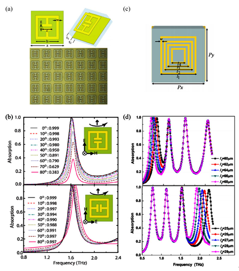
Fig. 1. Terahertz absorber based on metal-patch. (a) Schematic diagram of structure and (b) the absorption curve at different incident angles under TE and TM polarization of the terahertz metamaterial absorber based on three-layer structure proposed by Tao
et al [27];(c) Schematic diagram of structure and (d) the tunable changes of absorption curves depend on length
l1 and
l4 of the terahertz metamaterial absorber with multiband absorption proposed by Wang
et al [28] Fig. 2. Research history of tunable terahertz metamaterial absorber
[27, 29-33] Fig. 3. Single-band tunable terahertz metamaterial absorber. (a) Schematic diagram of structure and (b) the tunable changes of absorption curves depend on different Fermi energy level of the narrow band tunable terahertz absorber based on Dirac semi-metal proposed by Liu
et al [34]; (c) Schematic diagram of structure and (d) the tunable changes of absorption curves depend on different temperature and Fermi energy level of the tunable terahertz metamaterial absorber based on hybrid materials proposed by Huang
et al [35] Fig. 4. Multi-band tunable terahertz metamaterial absorber. (a) Schematic diagram of structure and (b) the tunable changes of absorption curves depend on different Fermi energy level of the double band tunable terahertz metamaterial absorber with five layers proposed by Chen
et al [50]; (c) Schematic diagram of structure and (d) the tunable changes of absorption curves depend on different Fermi energy level of the double band tunable terahertz absorber based on Dirac semi-metal proposed by Zhang
et al [51] Fig. 5. Broadband tunable terahertz metamaterial absorber. (a) Schematic diagram of structure and (b) the tunable changes of absorption curves depend on different conductivity of the narrow band tunable terahertz absorber based on vanadium oxide proposed by Song
et al [65]; (c) Schematic diagram of structure and (d) the tunable changes of absorption curves depend on different Fermi energy level of the wide band tunable terahertz absorber based on graphene proposed by Mou
et al [66] Fig. 6. Switchable bifunctional terahertz metamaterial absorber. (a) Schematic diagram of structure and (b) the tunable changes of absorption curves depend on different temperature of the double broadband switchable terahertz absorber proposed by Zhao
et al [32];(c) Schematic diagram of structure and (d) the tunable changes of absorption curves depend on different Fermi energy level of the wide band and narrow band switchable dual function terahertz absorber based on graphene and vanadium dioxide composite proposed by Zhang
et al [33]; (e) Schematic diagram of structure and (f) the tunable changes of absorption curves depend on different Fermi energy level of the switchable bifunctional terahertz absorber based on Dirac semi metal and vanadium dioxide proposed by Li
et al [85] | Layer | Material | Parameter | Fequency | Absorptance | Function | Reference |
|---|
| 3 | Graphene | Ef : 0~0.6 eV | 0.48~1.579 THz | >99% | Single-band tunable terahertz metamaterial absorber | [36] | | 3 | Dirac semimetal | Ef : 65~85 meV | 2.46~3.16 THz | >95% | [37] | | 4 | Dirac semimetal Strontium titanate | Ef : 10~80 meV T: 300 K | 3.265~4.82 THz | 70%~99.9% | [38] | T: 200~300 K Ef =40 meV | 2.665~3.69 THz | >99% | | 3 | Strontium titanate | T: 200~400 K | 1.71~2.48 THz | >99% | [39] | | 7 | Liquid crystal | V: 0~saturation | red shift | >90% | [40] | | 4 | InSb | T: 160~350 K | 0.82~1.02 THz | >88.7% | [41] | | 3 | Photoconductive silicon | σ: 1~1×10⁵ S/m | | 0%~100% | [42] |
|
Table 1. Summary of single-band tunable terahertz metamaterial absorber
| Layer | Material | Parameter | Frequency | Absorptance | Function | Reference |
|---|
| 3 | Graphene | Ef : 0.6~0.9 eV | 7.1~8.7 THz 10.4~12.7 THz | >85% | Dual-band absorption | [52] |
|---|
| 3 | Dirac semimetal VO2 | σ: 10~105 S/m Ef =0.13 eV | | 6.5%~97.8% 10%~99.27% 9%~99.54% | Triple-band absorption | [53] | Ef : 0.11~0.15 eV σ=105 S/m | blue shift | >90% | | 3 | Strontium titanate | T: 200~500 K | blue shift | >95% | Dual-band absorption | [54] | | 7 | Liquid crystal | V: 0~12 V | red shift | >80.1% | Dual-band absorption | [55] |
|
Table 2. Summary of multi-band tunable terahertz metamaterial absorber
| Layer | Material | Parameter | Frequency | Absorptance | Function | Reference |
|---|
| 4 | Dirac semimetal Strontium titanate | Ef : 40~0 meV T=300 K | unchanged 1.43~1.58 THz | >80% | BW=0.65 THz (absorptance>80%) | [67] | T: 250~400 K Ef =45 meV | 1.14~1.35 THz 1.51~1.76 THz | >80% | | 3 | Graphene | Ef : 0~0.7 eV | | 1%~99% | BW=0.76 THz (absorptance>90%) | [68] | | 3 | Graphene Graphene | Ef : 0.6~1.0 eV | 3.35~4.15 THz | >70% | BW=1.13 THz (absorptance>90%) | [69] | | 5 | Ef : 0.7~1.1 eV | 2.86~5.08 THz ~ 3.16~6.01 THz | >85% | BW=2.85 THz (absorptance>90%) | | 4 | Graphene VO2 | σ: 10~2×10⁵ S/m Ef =0.1 eV | | 28%~99% | BW=1.70 THz (absorptance>90%) | [70] | Ef : 0.1~0.6 eV σ=2×10⁵ S/m | Blue shift | >90% | | 3 | Dirac semimetal | Ef : 40~80 meV | Blue shift | | BW=2.70 THz (absorptance>90%) | [71] | | 3 | VO2 | σ: 200~2×10⁵ S/m | | 4%~100% | BW=4.10 THz (absorptance>90%) | [64] | | 5 | Graphene Dirac semimetal | Ef : 0 ~1.7 eV Ef = 60 meV | 5~7.44 THz ~ 4.79~8.99 THz | >80% | BW=4.20 THz (absorptance>90%) | [72] | Ef : 10~100 meV Ef =1.7 eV | Blue shift | |
|
Table 3. Summary of broadband tunable terahertz metamaterial absorber
| Layer | Material | Parameter | Frequency | Absorptance | Function | Reference |
|---|
| 6 | VO2 | σ: 0~105 S/m | | | Narrowband absorption switch to broadband absorption | [86] | | 5 | Graphene VO2 | σ: 40~2×10⁵ S/m Ef= 0.7 eV | | | broadband absorption switch to triple-band absorption | [87] | Ef : 0~0.7 eV σ= 40 S/m | | 20%~100% | BW=1.52 THz(absorptance>90%) | Ef : 0.5~1.0 eV σ=2×10⁵ S/m | 1~1.1 THz 2.2~2.65 THz 2.55~3.16 THz | >90% | triple-band absorption | | 6 | Graphene VO2 | σ: 200~2×10⁵ S/m Ef= 0.9 eV | | | six-band absorption switch to broadband absorption | [88] | | σ=2×10⁵ S/m | | >90% | BW=3.83 THz(absorptance>90%) | Ef : 0 eV~1.0 eV σ= 200 S/m | blue shift | >85.1% | six-band absorption | | 6 | Graphene VO2 | σ: 0 S/m~2×105 S/m Ef= 0.7 eV | | | broadband absorption switch to broadband absorption | [89] | | σ=2×10⁵ S/m | | >90% | BW=2.25 THz(absorptance>90%) | Ef : 0.01 eV~0.7 eV σ= 200 S/m | | 5.2%~99.8% | bandwidth=1.20 THz(absorptance>90%) | | 4 | Graphene | Ef : 150 meV~550 meV | | | broadband absorption switch to triple-band absorption | [90] | | 3 | Photoconductive silicon | σ: 1 S/m~5×105 S/m | red shift | | dual-band absorption switch to single-band absorption | [91] | | 5 | Photoconductive silicon VO2 | σ(Si): 2.5×10⁻⁴ S/m σ(VO2): 2×10⁵ S/m | | >90% | BW=4.66 THz(absorptance>90%) | [92] | σ(Si): 8×10⁴ S/m σ(VO2): 20 S/m | | >90% | dual-band absorption | σ(Si): 2.5×10⁻⁴~3×10⁵ S/m σ(VO2) =20 S/m | | 4%~99% | | σ(Si): 2.5×10⁻⁴~3×10⁵ S/m σ(VO2) =2×10⁵ S/m | | 60%~99% | | σ(VO2): 20~2×10⁵ S/m σ(Si) =2.5×10⁻⁴ S/m | | 2%~99% | | σ(VO2): 20~2×10⁵ S/m σ(Si) =8×10⁴ S/m | | 69%~99% | |
|
Table 4. Summary of switchable bifunctional terahertz metamaterial absorber
![Terahertz absorber based on metal-patch. (a) Schematic diagram of structure and (b) the absorption curve at different incident angles under TE and TM polarization of the terahertz metamaterial absorber based on three-layer structure proposed by Tao et al [27];(c) Schematic diagram of structure and (d) the tunable changes of absorption curves depend on length l1 and l4 of the terahertz metamaterial absorber with multiband absorption proposed by Wang et al [28]](/richHtml/lzdz/2023/40/3/301/img_01.jpg)
![Research history of tunable terahertz metamaterial absorber[27, 29-33]](/richHtml/lzdz/2023/40/3/301/img_02.jpg)
