• Chinese Optics Letters
  • Vol. 19, Issue 12, 121601 (2021)
Lulin Wei1, Jie Li1, Haohao Wang1, Shuhong Nie2, Wenming Su2, Dafang Huang1、*, and Mingwei Zhu1、**
Author Affiliations
  • 1National Laboratory of Solid State Microstructures & Jiangsu Key Laboratory of Artificial Functional Materials & College of Engineering and Applied Sciences, Nanjing University, Nanjing 210093, China
  • 2Suzhou Institute of Nano-Tech and Nano-Bionics, Chinese Academy of Sciences (CAS), Suzhou 215123, China
  • show less
    DOI: 10.3788/COL202119.121601 Cite this Article Set citation alerts
    Lulin Wei, Jie Li, Haohao Wang, Shuhong Nie, Wenming Su, Dafang Huang, Mingwei Zhu. Ultra-fast and low-cost fabrication of transparent paper[J]. Chinese Optics Letters, 2021, 19(12): 121601 Copy Citation Text show less
    Schematic of the rapid, universal fabrication process of transparent paper using different plants by lignin removal and cold pressing. (a) Taking the wood cell profile model as an example, plant cell walls have similar microstructures. Plant walls such as vine, bush, wood, bamboo, straw, branch, wheat, and other common plants have similar microstructures. The plant is (b) separated into small pieces and (c) delignified by NaClO subsequently. (d) Transparent paper achieved by cold pressing finally.
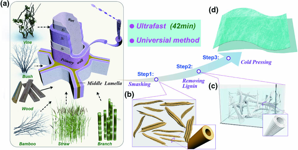
    Fig. 1. Schematic of the rapid, universal fabrication process of transparent paper using different plants by lignin removal and cold pressing. (a) Taking the wood cell profile model as an example, plant cell walls have similar microstructures. Plant walls such as vine, bush, wood, bamboo, straw, branch, wheat, and other common plants have similar microstructures. The plant is (b) separated into small pieces and (c) delignified by NaClO subsequently. (d) Transparent paper achieved by cold pressing finally.
    Take wood as an example to show the preparation process of transparent paper and the microstructure changes of corresponding materials. (a)–(d) Photos of the main processes of typical transparent paper fabrication and (e)–(h) the corresponding microstructure changes. (i) XRD profiles of wood chips and wood transparent paper, showing its main component of cellulose I, where 2θ of 16.5° and 22.5° correspond to the (110) and (200) planes of the cellulose crystal, respectively. (j) Nanofibrils with a diameter of about 30 nm in the wood cell. (k) AFM photo of transparent paper and the nanofibers can be observed.
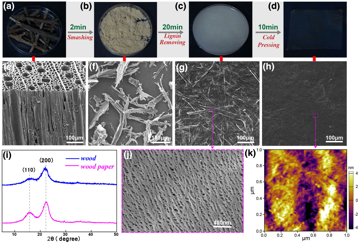
    Fig. 2. Take wood as an example to show the preparation process of transparent paper and the microstructure changes of corresponding materials. (a)–(d) Photos of the main processes of typical transparent paper fabrication and (e)–(h) the corresponding microstructure changes. (i) XRD profiles of wood chips and wood transparent paper, showing its main component of cellulose I, where 2θ of 16.5° and 22.5° correspond to the (110) and (200) planes of the cellulose crystal, respectively. (j) Nanofibrils with a diameter of about 30 nm in the wood cell. (k) AFM photo of transparent paper and the nanofibers can be observed.
    Excellent homogeneous optical and mechanical properties of transparent paper. (a) Transmittance and haze of the transparent paper with a thickness of about 50 µm. The inset shows that the school badge underneath the transparent paper made of bamboo is clearly seen. (b) Transmittance and haze of different nine points on a piece of wood transparent paper. (c) Graph of the 3D scattered light intensity, showing light is scattered in an isotropic manner. (d) Tensile stress-strain curve for bamboo transparent paper.
    Fig. 3. Excellent homogeneous optical and mechanical properties of transparent paper. (a) Transmittance and haze of the transparent paper with a thickness of about 50 µm. The inset shows that the school badge underneath the transparent paper made of bamboo is clearly seen. (b) Transmittance and haze of different nine points on a piece of wood transparent paper. (c) Graph of the 3D scattered light intensity, showing light is scattered in an isotropic manner. (d) Tensile stress-strain curve for bamboo transparent paper.
    Demonstration of transparent paper with good biodegradability, high temperature, and water stability as the substrate for electronic device. (a) Photos of transparent paper: (i) photo in grass soil and (ii) photo of it after 41 days. (b) (i)–(iii) Photos of original transparent paper and paper after treatment of high temperature and immersing chemical solvent, respectively. The paper was unchanged, after continuous treatment above. (b) (iv)–(vi) In contrast, PE deformed and solved after treatment of high temperature and chemical treatment, respectively, and (b) (vii)–(xi) PET crystallized and swelled after treatment of high temperature and chemical treatment, respectively. (c) (i), (ii) Transparent paper also can be bendable and foldable. (d) The bamboo transparent paper as printed circuit substrate. (d) (i)–(iii) Photos of original transparent paper with printed circuit and paper after treatment of high temperature and immersing chemical solvent, respectively. The circuit showed good conductivity. (d) (iv)–(vi) The microscope photos, correspondingly, after water and high-temperature treatment.
    Fig. 4. Demonstration of transparent paper with good biodegradability, high temperature, and water stability as the substrate for electronic device. (a) Photos of transparent paper: (i) photo in grass soil and (ii) photo of it after 41 days. (b) (i)–(iii) Photos of original transparent paper and paper after treatment of high temperature and immersing chemical solvent, respectively. The paper was unchanged, after continuous treatment above. (b) (iv)–(vi) In contrast, PE deformed and solved after treatment of high temperature and chemical treatment, respectively, and (b) (vii)–(xi) PET crystallized and swelled after treatment of high temperature and chemical treatment, respectively. (c) (i), (ii) Transparent paper also can be bendable and foldable. (d) The bamboo transparent paper as printed circuit substrate. (d) (i)–(iii) Photos of original transparent paper with printed circuit and paper after treatment of high temperature and immersing chemical solvent, respectively. The circuit showed good conductivity. (d) (iv)–(vi) The microscope photos, correspondingly, after water and high-temperature treatment.
    Lulin Wei, Jie Li, Haohao Wang, Shuhong Nie, Wenming Su, Dafang Huang, Mingwei Zhu. Ultra-fast and low-cost fabrication of transparent paper[J]. Chinese Optics Letters, 2021, 19(12): 121601
    Download Citation