1School of Science, Advanced Functional Material and Photoelectric Technology Research Institution, Hubei University of Automotive Technology, Shiyan 442002, China
2School of Science, Hubei University of Automotive Technology, Shiyan 442002, China
Yuan Zhou, Dong-Yan Lü, Wei-You Zeng, "Chiral single-photon switch-assisted quantum logic gate with a nitrogen-vacancy center in a hybrid system," Photonics Res. 9, 405 (2021)
Copy Citation Text
We propose what we believe is a novel proposal for realizing a quantum C-NOT logic gate, through fabricating an interesting hybrid device with a chiral photon-pulse switch, a single nitrogen-vacancy (NV) center, and an optical microcavity. Three major different practical routes on realizing a chiral photon emitter are discussed, which can implement a chiral control unit via the nonreciprocal emitter–photon interactions, so-called “propagation-direction-dependent” emission. With the assistance of dichromatic microwave driving fields, we carry out the relevant C-NOT operations by engineering the interactions on a single NV spin in a cavity. We note that this logic gate is robust against practical noise and experimental imperfection, and this attempt may evoke wide and fruitful applications in quantum information processing.
1. INTRODUCTION
In the quantum optics research area, it has always been a central goal to develop techniques for complete control of light–matter interaction at the single-quantum level, which underlies the essential physics of many phenomena and applications [1,2]. With the rapid innovation of the advanced photonic nanomaterials and processing technologies, a new quantum revolution on optics and photonics is accelerating the progress of the development for quantum information processing (QIP) [3–7].
Recently, “chiral quantum optics,” which leads to a chiral light–matter interaction, so-called “propagation-direction-dependent” emission, has quickly attracted widespread attention [8]. Utilizing this kind of chiral interface, we can constitute an interesting quantum control of photon–emitter interaction, such as the nonreciprocal interaction [9–20]. This new research can undoubtedly provide us with fundamentally new applications and functionalities in the area of quantum physics [21–23]. Moreover, we can fabricate a hybrid quantum system with this exciting photon–emitter setup to functionalize some special quantum operations [24,25]. Perhaps this hybrid system with the chiral units can become a key resource for QIP in the near future [26,27].
As a point defect in diamond, the nitrogen vacancy (NV) centers integrated in a hybrid quantum system have recently emerged as one of the leading candidates for QIP thanks to their excellent spin properties, such as atom-like properties, solid-state spins without any trap, easy scalability, and longer coherence time even at ambient conditions [28–30]. Significant theoretical and experimental investigations have been carried out to realize quantum simulation and manipulation [31–40]. It is still a challenge to control a single NV center with enough strength at single-quantum level in the microwave-frequency domain, and this is also a serious limitation for its wide application in QIP [41–46]. However, in the optical-frequency domain, we can conveniently fabricate the NV center with the optical cavity or optical lattice in a hybrid device, and coherently manipulate the NV center at single-quantum level with enough strong coupling [47–52]. QIP with integrated photonics has attracted much attention recently [53]. It was also studied in Ref. [54] with the linear combination of unitary architecture [55]. QIP based on an NV center and optical microcavity was also studied in Ref. [56]. Progress in the fabrication and application of optical microcavity is reviewed in Ref. [57], and propagation-direction-dependent emission is reviewed in Ref. [58]. This efficient and reliable optical interface indicates to us a promising direction for studying the NV centers in QIP [56].
Sign up for Photonics Research TOC. Get the latest issue of Photonics Research delivered right to you!Sign up now
In this work, we propose realizing a robust quantum C-NOT logic gate [59] by fabricating a single NV center, an optical microcavity, and a chiral photon-pulse switch in a hybrid device. Here, we stress that we can implement an exquisite chiral control unit via three major different routes. For the first route, we can apply the idea of the nonreciprocal atom–photon or spin–photon interaction to realize this chiral control unit, called a “one-atom router” [9,48,60]. Second, according to the recent achievement on emitting the path-encoded photon utilizing an in-plane spin–photon interface accomplished by the I. J. Luxmoore group; we can also apply the quantum dot (QD) system to realize this chiral photon switch [11]. The third practicable route is to apply the surface plasmon (SP) scheme to realize this chiral photon emitter, in which the representative research comes from the M. D. Lukin group and the H. X. Xu group [13–15]. As these propagation-direction-dependent emitters will deliver the mode optical pulse into the optical microcavity and reflect or filter the mode out in a well-controlled setup, we can achieve a series of relevant C-NOT operations by engineering the interactions of a single NV center in an optical microcavity or optical lattice, with the assistance of dichromatic microwave driving fields. In this scheme, we have not only made the analytical discussions, but also carried out the numerical simulations with the cavity dissipation, the NV decay and dephasing, and the system dispersion all being considered. We stress that this proposal may provide us with a quantum C-NOT gate with high fidelity that is also robust against practical noise and experimental imperfection, even under realistic conditions. We also hope it may be a scalable and universal proposal for the realistic QIP in the near future.
This paper is organized as follows. In Section 2, we introduce the scheme and the basic idea for this hybrid setup; in Section 3, we introduce the basic theoretical mechanism for this scheme. The relevant C-NOT operation matrix analysis of this scheme is discussed in Section 4, and the relevant numerical simulations are carried out in Section 5 by solving the whole-system master equation. In Section 6, we discuss the effect on this scheme caused by system imperfections. Finally, we study the relevant experiment parameters of this setup according to the current experimental advancement in Section 7 and make a brief conclusion on this work in the last section.
2. SCHEME
The traditional C-NOT gate can be described by the unitary operator, where and stand for two general orthogonal quantum states of the control unit, which, respectively, mean “Yes” or “No,” or mean the switch is “On” or “Off.” We can model this control unit in plenty of different setups, such as light with polarization, atom, ion or artificial atom with two-level states, or chiral light [61–66]. In Eq. (1), and are, respectively, the identity matrix and the Pauli matrix -component for a qubit.
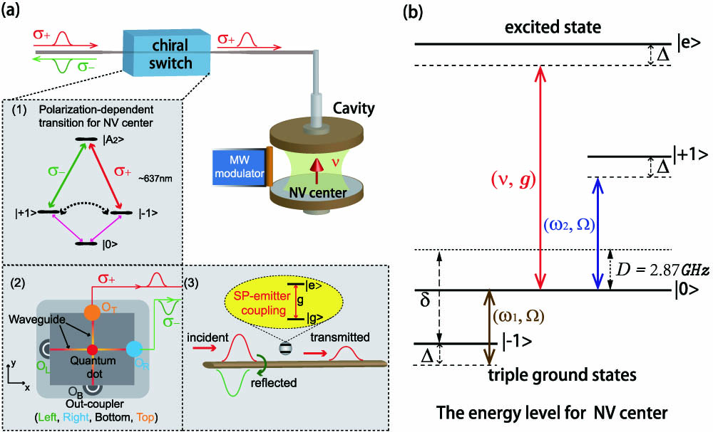
Figure 1.Scheme diagrams. (a) This hybrid device consists of two parts, a chiral switch for emitting photon pulse and an optical microcavity embedded with a single NV center, both of which are connected with an optical nanofiber. The outputs are delivered to the optical microcavity through nanofiber. A single NV center, driven by a dichromatic microwave field, is planted in the optical microcavity, which will also interact with the optical modes near-resonantly. (b) Level diagram of the NV center ground triplet state and excited state, and the feasible transition channels. The brown and blue solid arrows indicate the dichromatic microwave driving fields (with frequencies and , and Rabi frequencies and ) applied between the state and the state . The red solid arrows indicate the optical transition between the state and the excited state , which is induced by modes.
In this work, our goal is to achieve a novel chiral C-NOT gate by engineering the quantum states of a single electronic spin through exquisite tailoring spin-photon interactions [67,68]. To make sure of the implementation of this logic gate, we should accomplish two major procedures: (i) the control unit and (ii) the C-NOT operation kernel in this project. Here, we first stress that this proposal can only work well at cryogenic temperatures, and we have illustrated a feasible scheme on this proposal in Figs. 1(a) and 1(b). Then we can make a detailed analysis. For the first procedure, we need to present a well-controlled switch for emitting a photon pulse. Here, we take advantage of propagation-direction-dependent emission in the research field of chiral quantum optics [8]. In recent years, with the rapid development of advanced photonic nanostructures, this exciting physics has been realized within different experimental facilities [8,9,11,13–20]. Basing this work on these advanced achievements, we apply three major different routes for realizing a well-controlled optical routing to functionalize a chiral photon-pulse switch. All of them are plotted in Fig. 1(a), which includes setups (1), (2), and (3), respectively.
As illustrated in Fig. 1(a), realizing this chiral switch, three major different routes are considered in this work. The first potential route is illustrated in Fig. 1(a) [Scheme (1)]. In this scheme, we utilize M. D. Lukin group’s achievement on implementing the quantum entanglement between the polarization of a single optical photon and an NV center [48]. Therefore, this type of polarization-dependent optical transition indicates that we can implement a more feasible single-photon chiral switch by means of this polarization technology. Perhaps the I. Shomroni group may provide us with another interesting method for realizing this chiral switch, which is composed of a chip-based silica whispering-gallery-mode (WGM) microresonator (MR) that is strongly and magnetically coupled to a single atom [8,9,60]. By comparing these two types of methods, we believe that the one plotted in Scheme (1) may be more suitable for this system.
To realize this single-photon chiral switch, the details of this so-called optical polarization manipulation and selection are as follows [48]. As shown in setup (1), the NV center in diamond with a high purity plays the role of the polarized light source, and its chiral emission can be controlled by the MW signals conveniently. Specifically, the NV center prepared in a specific excited state will decay into two different long-lived spin states by the emission of orthogonally polarized optical photons with the wavelength 637 nm and the polarization owing to total angular momentum conservation. For instance, the state decays to the ground state through polarized radiation and to state through polarized radiation. At first, we can initialize the NV into the ground state with the off-resonant 532 nm laser, and then accurately manipulate the populations of the states and in time through the MW control. So, we can reach the goal of the implementation of a chiral photon emitter. Furthermore, in order to improve the efficiency of this chiral switch for emitting the determinately polarized photons into the cavity or not, we can also apply the general polarization filter to connect the chiral switch and the cavity. Therefore, we can achieve the basic goal: mode photons are transmitted into the cavity, while the photons of the mode are rare and filtered out. According to the relevant experimental report, we consider that the fidelity of this chiral switch for emitting and transmitting the mode photons into the cavity will reach more than 90% [48].
Setup (2) means the recent achievement on emitting the path-encoded photon utilizing an in-plane spin-photon interface accomplished by the I. J. Luxmoore group; we can also apply this type QD system to realize this chiral switch [11]. In this spin to the guided photon interface, the QD located at the center of the waveguide intersection will coherently emit the ()-polarization component of a circularly polarized state into the waveguides aligned along the () direction, respectively. By collecting both polarization components while retaining their relative phase, the full polarization state of the photon is mapped to a path-encoded state; then we can implement a more feasible chiral switch by means of the polarization technology.
In setup (3), we can also apply the SP scheme to realize this chiral photon emitter, and these representative achievements come from the M. D. Lukin group and the H. X. Xu group [13–15].
Furthermore, many other feasible schemes can also be applied to realize this type of chiral switch equivalently in this work [16–20,58]. Therefore, for realizing the chiral control unit in this scheme, we can utilize many equivalent schemes to make this procedure function. Based on this type of nonreciprocal interaction in the different setups above, we can realize a well-controlled chiral photon-pulse switch, the so-called propagation-direction-dependent emitter. As a result, for this procedure, the photons with mode can be delivered into the cavity to drive the NV spin, while the photons with mode will be reflected away.The second procedure is to provide a more reliable operation kernel (atom or artificial atom) to implement this logic gate operation more conveniently. Among all different quantum systems, NV centers in diamond are particularly attractive due to their excellent spin properties, even at ambient conditions. Especially, hybrid systems based on NV centers are reliable and promising setups for QIP due to their easy scalability and longer coherence time. As illustrated in Fig. 1(a), we consider a single NV center embedded in an optical microcavity. The input of the cavity is connected to the chiral switch of photon pulse through a nanofiber. So, the input signal ( single-photon pulse) will induce the resonant transition from state to the excited states with assistance of the cavity mode . The energy level structure of a single NV center is shown in Fig. 1(b). Here we choose one of its excited states as the unique excited state . The electronic ground triplet state is the eigenstate of spin operator with , and the zero-field splitting between the degenerate sublevels and is .
As we know, this photon pulse into the cavity may induce multiple and complex optical transitions between the triple ground states and the multilevel excited states. With the purpose of reducing these transitions to and discarding the optical transitions between and the other excited states, we can apply a strong homogeneous static magnetic field to remove the degenerate states with Zeeman splitting . Due to the far detuning condition , we can discard these unnecessary transitions and reduce NV to the unique optical transition, . As a result, this unique optical transition with interaction is described as () , with the coupling strength and the fundamental frequency . Meanwhile, we introduce tunable dichromatic microwave driving fields to drive the transitions between states and . So, the Hamiltonian for describing these interactions is , with the tunable oscillating frequencies and and Rabi frequencies . The energy-level transitions for this scheme are also plotted in Fig. 1(b); the red solid arrow indicates the optical transition between the state and the excited state , which is induced by modes; the brown and blue solid arrows indicate the ground-state transitions between the states and , respectively.
3. BASIC THEORETICAL MECHANISM
Although this propagation-direction-dependent emitter is the key point of this chiral switch for realizing the quantum C-NOT gate, we can conveniently implement the control of the photon-pulse signal delivered into the cavity or not through different setups for this scheme. Here, we stress that the following two opposite cases should be taken into consideration. For Case (I), this chiral switch delivers a single-photon pulse ( photon) into the optical microcavity, which will induce the optical transition between the states and , and then we can make the definition as for this control unit, while for Case (II), the incoming photon signal cannot be delivered into this cavity owing to this chiral switch; then, we can also define for this control unit. The photon is delivered into the cavity to interact with the NV center and the control unit is , the so-called “Off” state. Then we can obtain the Hamiltonian in the Schrödinger picture (SP) for this operation unit as follows:
Here, the three items in Eq. (2) above are, respectively, , , and . The first item, , is the free Hamiltonian for describing the single NV center, the second item, , characterizes the interaction between an NV electronic spin and the optical cavity, and the last item, , stands for the dichromatic microwave driving fields acting on the NV center with the ground-state transitions .
Then we apply a frame rotation (based on ) and a transformation of representation [] to Eq. (2). We can then obtain the equivalent expression in the interaction picture (IP), where the corresponding detunings satisfy the relations . Discarding the energy shift item , we can then achieve the effective Hamiltonian under the condition of large detuning (), with , , and . To make it easier, here we have isolated a subsystem comprising , where denotes the state of cavity mode with only one (no) photon. Through solving the Schrödinger equation , we can get two different dark states, and , with the eigenvalue .
Here in this scheme, we assume , and the dark state . During this dynamical evolution process according to , we find the following rules. Once the photon and NV center are initially prepared in , the system will undergo the dynamical evolution that follows the unique linear superposition of dark states and with expression . On the contrary, when the initial state is , another superposition will be the unique target state for its evolution. As a result, for Case (I) we have realized a controlled invariant operation: , in which the control unit chiral switch is in the “Off” state (Appendix A). The photon is reflected away by this chiral switch, and no photon is delivered into the cavity. Therefore, the control unit is turned to state , the so-called “On” state. Meanwhile, the triple ground-state transition of the NV center is always maintained by this classical dichromatic microwave field. So, we can describe the Hamiltonian in the SP as follows:
In the same way, we can get the Hamiltonian with equivalent expression in the IP, where the corresponding detunings satisfy the relations . Then we can also achieve the effective Hamiltonian under the condition of large detuning (),
According to Eq. (7), we find that will undergo the state transition to each other () at the time of (). Therefore, for Case (II), we also have realized the spin-flip operation, which is also controlled by this chiral switch in the “On” state.
In a word, utilizing a chiral photon-pulse switch controlled by this nonreciprocal interaction, we can realize a complete quantum C-NOT operation with an NV center in this hybrid system.
4. C-NOT OPERATION MATRIX OF THIS SCHEME
To indicate this C-NOT logic operation process more clearly, we apply the relevant controlled operation gate matrices to our scheme [59]. Considering Eq. (1), the ideal C-NOT gate matrix can be expressed as in which, the upper left quadrant and lower right quadrant correspond to the identity matrix and inversion matrix , respectively.
In contrast to J. H. Plantenberg and J. E. Mooij group’s two-qubit C-NOT experimental demonstration [59], the major difference in this work is that the control unit (chiral switch) is independent of the operation qubit (NV spin); perhaps we may call it the single-qubit controlled C-NOT operation. This bichromatic drive is also independent of the state of the control unit (the chiral switch) in this scheme. During the whole controlled C-NOT operation in this scheme, the microwave bichromatic driving fields are always acting on the NV spins in both cases.
In Case (I), the mode photon is transmitted into the cavity, and we can obtain the identity operation approximately with the relation . Here, we can describe this effective operation as with when . For Case (II), there is no photon inside the cavity, and the microwave bichromatic driving fields dominate this inversion operation, which corresponds to the C-NOT operation of the NV spin. Here we stress that this inversion operation is a dynamical periodic process, and we can apply the universal method of the two-level Bloch sphere to express this operation equivalently [59]. For this operation unit matrix, we can add an additional single-qubit z-rotation with , which can ensure us the real inversion operation matrix . According to Eq. (7), this matrix can be expressed as with the effective coupling . Combining the two cases above, we can rewrite this whole C-NOT operation matrix as
Therefore, discarding the system dissipation and dispersion, we can obtain with the condition of and . To quantify the basic fidelity of the scheme, we can utilize the definition [59]. Then we can get
5. NUMERICAL SIMULATIONS
To confirm the analysis results discussed above, let us make the corresponding numerical simulations to further exhibit the feasibility of this scheme. In general, for this proposal, this hybrid quantum system satisfies the whole dynamical evolution, which is dominated by the master equation,
In Eq. (13), is the density operator, including the freedom of cavity mode and NV center. and mean two different Hamiltonians for Case (I) and Case (II), respectively. We define an operator as , and apply to describe the dissipation rate of the optical microcavity. Here, is the NV center’s average decay rate induced by the spontaneous emission from excited state to the ground states. For a single NV center, considering all of the spontaneous emission channels (such as and ), dominates this decay process with the highest probability. By utilizing this property, one can initialize the NV center to the state conveniently. By discarding the other two weak transitions, we assume . In addition, we also apply to describe the NV center’s dephasing rate for this type of ground-state electron spin. In fact, this effect is mainly caused by the interactions from the crystal strain and the other adjacent electron spins or nuclear spins, so we define .
Figure 2.For Case (I), the dynamical evolution of the fidelity, (a) and (b) with the initial state , and (c) and (d) with the initial state , in which (a) and (c) correspond to the dynamical fidelity versus the coupling strength , with the coefficients , , , , and ; (b) and (d) correspond to the dynamical fidelity versus the detuning , with the coefficients , , , , and .
Figure 3.For Case (II), the dynamical evolution of the fidelity, with the initial state and the coefficients , , , and , in which the solid gray line with the hollow square shows the fidelity of , the solid blue line with the open circle shows the fidelity of , and the solid red line with the hollow diamond shows the fidelity of .
According to the simulation results for these two different cases above, we find that, in this proposal, we can not only perform the invariant operation with a high fidelity, so called operation, but also realize a well-controlled spin-flip operation, so-called operation. These results above also indicate that we can implement a complete quantum C-NOT logic gate with high fidelity.
6. EXPERIMENTAL IMPERFECTIONS
We now discuss the experimental imperfections. In this scheme, the experimental imperfections are mainly focused on the physical dispersion of the dichromatic microwave driving fields with the Rabi frequencies and oscillating frequencies . As we have utilized the two-photon Raman transition process with the constraint of large detuning, a little change in each oscillating frequency or will not induce a significant impact on our scheme. So, there is no doubt about us discarding this possible dispersion factor.
However, we cannot guarantee these two Rabi frequencies are exactly the same in the realistic demonstration of this scheme. Considering this possible factor, we can rewrite the Hamiltonian in Eqs. (2) and (5) with the expression,
Here, we assume and , with . The dispersion factor is defined as , with .
Figure 4.For Case (I), (a) and (b) the dynamical fidelity of state transitions versus the dispersion , with the coefficients , , , , and , while for Case (II), (c) and (d) the dynamical fidelity of states and during the process of state transitions , versus the dispersion , with the coefficients , , , and .
For Case (I), the results are illustrated in Figs. 4(a) and 4(b), with the coefficients , , , , and . We can implement the state transitions with high fidelity of more than 0.94, when the dispersion satisfies , while for Case (II), the results are also illustrated in Figs. 4(c) and 4(d), with the coefficients , , , and . These results show that we can accurately realize the spin-flip operation () with a fidelity near to unity. However, for the spin-flip time , this dispersion factor will inevitably cause a increasing time displacement on it as we increase the dispersion rate. In this scheme, we think there are two routes for us to manage this problem. The first route is to modulate the detuning by adjusting the static magnetic field, which induces the Zeeman splitting of the ground states . Then we can revise the parameter to the value without a dispersion factor. Another route is to recalibrate the evolution time for this hybrid system. These simulation results, accompanied with the experimental imperfection conditions, show that this scheme has strong fault tolerance.
Figure 5.The estimation of the average fidelity for this whole C-NOT operation process versus the dispersion rate , in which, the black line with the open square means the average fidelity of the controlled spin-invariant operation, the red line with the open circle means the average fidelity of the controlled spin-flip operation, the blue line with the open up triangle means the whole average fidelity of this C-NOT operation, and the violet line with open down triangle means the whole average fidelity of the C-NOT operation accompanied with the realistic chiral switch efficiency (estimated as ). The parameters are assumed as , , , and .
To examine the feasibility of our scheme in a realistic experiment, we now discuss the relevant experimental parameters. We first stress that this proposal can only work well at cryogenic temperatures during this whole scheme. According to the recent investigations and achievements on implementing a propagation-direction-dependent emitter, we can take advantage of these setups as our chiral photon-pulse switch for this proposal, with the efficiency of [9,11,13–20]. With the rapid development of advanced fabrication and nanotechnology and according to the recent achievements on fabricating a high-quality optical cavity with advanced nanomaterials and processing technology, we can suppose that the quality of the optical cavity in this theoretical work satisfies [73–76]. Compared with its intrinsic frequency , we can assume its decay rate as MHz in which the coupling strength for the single NV center will reach near [47–51]. The Rabi frequency for this dichromatic microwave driving fields is tunable, and we can assume .
Here we stress that there are two essential steps for realizing this C-NOT operation completely in this scheme. For the first step, once the photon is transmitted into the cavity, we can implement the invariant operation (unit matrix ) by means of optical waves and dichromatic microwaves. Once no photon exists in the cavity, then we can implement this second-step reversal operation (NOT gate ) only through manipulating its ground states by this original dichromatic microwave. During this process, we can maintain the invariant operation in a short period (10 ns), but the reversal operation needs a much longer time (μ) to finish. However, the reversal operation procedure is independent of its excited state or the optical domain. Therefore, in this order, we think the limitation of lifetime or coherence time for the excited state will not affect this second-step operation. While we exchange the order of these two steps, and the first step is the reversal operation, we have to finish this reversal operation first in a long period. After that, the coherence of the excited state vanishes early, so we need to initialize this setup again to ensure that the coherence time of the excited state is enough to implement another step: invariant operation.
The relaxation time of the NV center ranges from milliseconds to several seconds; an even longer time has been reported; however, the dephasing rate plays a kernel role in limiting its coherence time [77–79]. In fact, the decoherence will be dominated by the hyperfine interaction with the nuclear spins, which mainly form the nuclear spin bath. [In general, the single NV spin decoherence in diamond is mainly caused by the coupling of the surrounding electron or nuclear spins, such as the electron spins P1 centers, the nuclear spins spins and spins. In Type Ib diamond samples, the free-induction decay of the NV spin in an electron spin bath (P1 centers) can be neglected, and in high-purity Type II samples, the decay time caused by the electron spin bath will exceed 1 ms. The coupling to the host nuclear spin induces the substantial coherent off-resonance errors, which have been solved experimentally.] With the development of dynamical decoupling techniques [80–89], the dephasing time of a single NV center in diamond can be more than 2 ms [90–93]. According to the parametric estimation of our scheme, we need at least tens of microseconds to accomplish the relevant coherent operations. Therefore, the coherence time is sufficient for us to accomplish this type of quantum logic gate.
8. CONCLUSION
In summary, by fabricating a hybrid device with a single NV center in an optical microcavity and a chiral photon-pulse switch, we have proposed a novel and efficient proposal for realizing a robust quantum C-NOT logic gate. In this scheme, we can implement the chiral control unit via several different setups, which will induce the propagation-direction-dependent photon emission. Then we can get a well-controlled switch for delivering the mode photon pulse into the optical microcavity and for reflecting or filtering out the mode. After that, we can achieve two steps of relevant C-NOT operations by engineering the interactions of the single NV center in the cavity with the assistance of dichromatic microwave driving fields. Taking the cavity dissipation, the NV decay and dephasing, the system dispersion, and even the efficiency of this chiral switch into our consideration, we also have carried out the analytical discussions and the numerical simulations of this scheme. In this theoretical attempt and during the whole dynamical operation, the primary adverse factors on destroying the fidelity are mainly focused on both decays of the cavity () and the excited state of the NV center (), and even the efficiency of this chiral switch (estimated as ). However, with the development of the advanced micronanofabrication technologies, we are full of confidence in the preparation of a higher quality cavity with in the near future. Applying other atoms (or artificial atoms) with a longer lifetime to this scheme may be a reasonable improvement as well. Although the realistic fidelity of this scheme is estimated as less than the achievement and results in Ref. [56], we still hope it will be a useful attempt for implementing quantum manipulation with integrated or hybrid optical quantum devices owing to its inherent innovative and interesting nature.
Acknowledgment
Acknowledgment. We thank Sheng-Li Ma and Guang-Hui Wang for the helpful discussions on this work. Part of the simulations are coded in PYTHON using the QUTIP library [94,95].
APPENDIX A: EIGEN SYSTEM OF HAMILTONIAN H^IP(I) and H^IP(II)
For Case (I), considering the Hamiltonian in Eq.?(3) of Section?3, we can rewrite this Hamiltonian with an equivalent expression,
Through solving the Schr?dinger equation , we can get its first dark state with . Then we can also write in the matrix form with its subspace , with its eigen energies and eigenstates in Table?1, in which we assume . On the other hand, we consider another Hamiltonian in Case (II) with an equivalent expression,
Eigen System of
Eigen Energy
Eigenstate
Therefore, we can also express in matrix form in its subspace ,
Its eigen energies and eigenstates are also plotted in Table?2, in which we also assume .
Yuan Zhou, Dong-Yan Lü, Wei-You Zeng, "Chiral single-photon switch-assisted quantum logic gate with a nitrogen-vacancy center in a hybrid system," Photonics Res. 9, 405 (2021)