• Acta Optica Sinica
  • Vol. 43, Issue 6, 0600001 (2023)
Zeliang Zhang, Pengfei Qi, Lanjun Guo, Nan Zhang, Lie Lin, and Weiwei Liu*
Author Affiliations
  • Tianjin Key Laboratory of Micro-Scale Optical Information Science and Technology, Institute of Modern Optics, Nankai University, Tianjin 300350, China
  • show less
    DOI: 10.3788/AOS221632 Cite this Article Set citation alerts
    Zeliang Zhang, Pengfei Qi, Lanjun Guo, Nan Zhang, Lie Lin, Weiwei Liu. Review on Super-Resolution Near-Field Terahertz Imaging Methods[J]. Acta Optica Sinica, 2023, 43(6): 0600001 Copy Citation Text show less
    Resolution range of THz near-field imaging based on aperture-probe and scattering probe and corresponding application scenarios
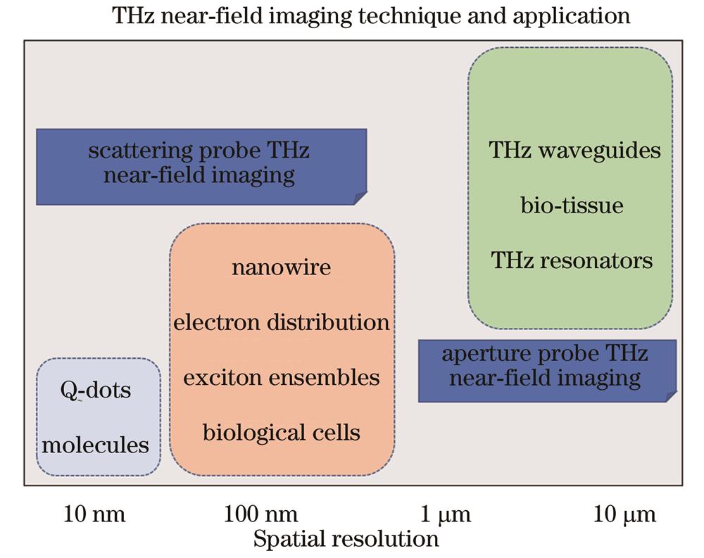
    Fig. 1. Resolution range of THz near-field imaging based on aperture-probe and scattering probe and corresponding application scenarios
    Schematic diagram of conical aperture experimental setup and its imaging results. (a) Experimental optical path of tapered THz waveguide[17]; (b) selection of THz wavelength by tapered waveguide (frequency spectrum width of taper waveguide is about 1 THz); (c) imaging effect of tapered waveguide on resolution plate
    Fig. 2. Schematic diagram of conical aperture experimental setup and its imaging results. (a) Experimental optical path of tapered THz waveguide[17]; (b) selection of THz wavelength by tapered waveguide (frequency spectrum width of taper waveguide is about 1 THz); (c) imaging effect of tapered waveguide on resolution plate
    Schematic diagrams of multiple physical aperture waveguides. (a)(b) Structures of semi-open tapered waveguides[18,20]; (c) picture of metal enclosed tapered waveguide[21]; (d) electric field distribution of tapered waveguide; (e) schematic of confocal THz waveguide; (f) imaging effect of confocal waveguide for resolution plate[19]
    Fig. 3. Schematic diagrams of multiple physical aperture waveguides. (a)(b) Structures of semi-open tapered waveguides[1820; (c) picture of metal enclosed tapered waveguide[21]; (d) electric field distribution of tapered waveguide; (e) schematic of confocal THz waveguide; (f) imaging effect of confocal waveguide for resolution plate[19]
    Bull's eye structure and its imaging effect[22]. (a) THz transmission spectrum of bull's eye structurefor specific wavelength; (b) sample of metal wires to be imaged; (c) imaging result for Fig. 4(b) obtained by bull's eye structure
    Fig. 4. Bull's eye structure and its imaging effect[22]. (a) THz transmission spectrum of bull's eye structurefor specific wavelength; (b) sample of metal wires to be imaged; (c) imaging result for Fig. 4(b) obtained by bull's eye structure
    Dynamic aperture THz near-field imaging. (a) THz near-field imaging system based on optical pump to control local carrier concentration (image on the right shows imaging effect of system on metal wires[23]); (b) dynamic aperture THz imaging system based on compressed sensing imaging technology (image on the right shows imaging effect of system on metal wires[26]); (c) dynamic aperture THz imaging system based on two-color femtosecond laser filament (image on the right is imaging effect of system on metal holes[27]); (d) THz near-field imaging system based on orthogonal double filaments (image on the right shows imaging effect of system on metal wire structure[28])
    Fig. 5. Dynamic aperture THz near-field imaging. (a) THz near-field imaging system based on optical pump to control local carrier concentration (image on the right shows imaging effect of system on metal wires[23]); (b) dynamic aperture THz imaging system based on compressed sensing imaging technology (image on the right shows imaging effect of system on metal wires[26]); (c) dynamic aperture THz imaging system based on two-color femtosecond laser filament (image on the right is imaging effect of system on metal holes[27]); (d) THz near-field imaging system based on orthogonal double filaments (image on the right shows imaging effect of system on metal wire structure[28])
    Plasmon focusing structures. (a) THz focusing period structure with metal cone[29]; (b) THz focusing period structure with Domino metal cone[30]; (c) superlens with metallic period structure[31]; (d) superlens with fan-shaped metallic period structure; (e) focused electric field distribution of Fig. 6(d)[33]; (f) imaging modeling effect of graphene surface plasmon for gold slit[36]; (g) electric field controlled conical graphene plasmon focusing structure; (h) principle of graphene superlens based on four wave mixing (image on the right is superlens focusing electric field distribution[38]); (i) calculated electric field effect of structure in Fig. 6(g)[37]
    Fig. 6. Plasmon focusing structures. (a) THz focusing period structure with metal cone[29]; (b) THz focusing period structure with Domino metal cone[30]; (c) superlens with metallic period structure[31]; (d) superlens with fan-shaped metallic period structure; (e) focused electric field distribution of Fig. 6(d)[33]; (f) imaging modeling effect of graphene surface plasmon for gold slit[36]; (g) electric field controlled conical graphene plasmon focusing structure; (h) principle of graphene superlens based on four wave mixing (image on the right is superlens focusing electric field distribution[38]); (i) calculated electric field effect of structure in Fig. 6(g)[37]
    Near-field antenna structures. (a) Structure diagram of single-band gap near-field antenna (distance between two metal wire tips is 1.8 μm, and right image shows scanning results of this near-field antenna for different incident THz polarization states[40]); (b) on-chip integrated aperture near-field THz antenna structure, and image on the right shows transmission signal of this antenna[41]; (c)(d) influence of incident light polarization on scanning results of near-field THz antennas[42]
    Fig. 7. Near-field antenna structures. (a) Structure diagram of single-band gap near-field antenna (distance between two metal wire tips is 1.8 μm, and right image shows scanning results of this near-field antenna for different incident THz polarization states[40]); (b) on-chip integrated aperture near-field THz antenna structure, and image on the right shows transmission signal of this antenna[41]; (c)(d) influence of incident light polarization on scanning results of near-field THz antennas[42]
    Scattering probe THz near-field imaging system[46]. (a) Schematic diagram of scattering probe THz near-field imaging (left image) and schematic diagram of incident pulse irradiating tip of needle and surface of sample (right picture)(Einc is incident signal, and Escat is scattering signal); (b) result of self-homodyne scheme; (c) result of quadrature homodyne scheme; (d) result of pseudoheterodyne scheme; (e) result of synthetic optical holography; (f) result of pseudoheterodyne scheme; (g) intensity curves and phase curves of single-scan THz near-field signal at dotted line positions in Figs. 8(b)-(f)
    Fig. 8. Scattering probe THz near-field imaging system[46]. (a) Schematic diagram of scattering probe THz near-field imaging (left image) and schematic diagram of incident pulse irradiating tip of needle and surface of sample (right picture)(Einc is incident signal, and Escat is scattering signal); (b) result of self-homodyne scheme; (c) result of quadrature homodyne scheme; (d) result of pseudoheterodyne scheme; (e) result of synthetic optical holography; (f) result of pseudoheterodyne scheme; (g) intensity curves and phase curves of single-scan THz near-field signal at dotted line positions in Figs. 8(b)-(f)
    Pseudoheterodyne detection scheme. (a) Experimental setup and schematic diagram of pseudoheterodyne detection[48] (following figure shows that extracted frequency of near-field signal is sum of higher order harmonics of probe vibration frequency and piezoelectric ceramic vibration frequency); (b) result of atomic force microscopy imaging; (c) result of pseudoheterodyne detection imaging; (d) result of homodyne detection image
    Fig. 9. Pseudoheterodyne detection scheme. (a) Experimental setup and schematic diagram of pseudoheterodyne detection[48] (following figure shows that extracted frequency of near-field signal is sum of higher order harmonics of probe vibration frequency and piezoelectric ceramic vibration frequency); (b) result of atomic force microscopy imaging; (c) result of pseudoheterodyne detection imaging; (d) result of homodyne detection image
    THz near-field imaging system based on scanning tunneling microscopy. (a) Imaging principle of THz scanning tunneling microscope [49]; (b) imaging effect of gold nanoparticles; (c) incident time-domain signal and corresponding spectrum; (d) time resolution of multilayer C60 on gold substrate[50]; (e) measurement process of ultrafast electron dynamics with sub-nanoscale spatial resolution and subcycle time resolution; (f) imaging result of scanning tunneling microscope; (g) near field time-domain signal[50]; (h)-(j) THz near field 2D scanning results after two-dimensional scanning of scanning tunneling microscope and THz assisted tunneling current enhancement[51]; (k) incident THz time-domain signal and corresponding spectrum[51]
    Fig. 10. THz near-field imaging system based on scanning tunneling microscopy. (a) Imaging principle of THz scanning tunneling microscope [49]; (b) imaging effect of gold nanoparticles; (c) incident time-domain signal and corresponding spectrum; (d) time resolution of multilayer C60 on gold substrate[50]; (e) measurement process of ultrafast electron dynamics with sub-nanoscale spatial resolution and subcycle time resolution; (f) imaging result of scanning tunneling microscope; (g) near field time-domain signal50; (h)-(j) THz near field 2D scanning results after two-dimensional scanning of scanning tunneling microscope and THz assisted tunneling current enhancement[51]; (k) incident THz time-domain signal and corresponding spectrum[51]
    Features of THz near-field imaging system based on atomic force microscopy. (a) THz near field time evolution under optical pump (right image is 2D scanning result, and imaging resolution is 10 nm); (b) time-domain curve and corresponding spectrum and phase of incident THz signal[53]; (c) imaging results of metal grating covered by thin film of dielectric material under three different electric field intensity; (d) time-domain curve and corresponding spectrum obtained by near field scattering measurement[54]
    Fig. 11. Features of THz near-field imaging system based on atomic force microscopy. (a) THz near field time evolution under optical pump (right image is 2D scanning result, and imaging resolution is 10 nm); (b) time-domain curve and corresponding spectrum and phase of incident THz signal[53]; (c) imaging results of metal grating covered by thin film of dielectric material under three different electric field intensity; (d) time-domain curve and corresponding spectrum obtained by near field scattering measurement[54]
    Effect comparison of THz near-field imaging system based on atomic force microscopy. (a) Result of atomic force microscopy imaging; (b) THz near field microscopy imaging result; (c) infrared near-field microscopy imaging result[55]; (d) atomic force microscopy image of gold disks; (e) THz near field microscopy image of gold disks; (f) ID scanning signal curves of THz near field microscopy; (g) two-order near-field scattering signal and calculated electric field curves at point charge for ungrounded and grounded disks, respectively[56]; (h)(i) results of local detection and unlocal detection; (j) 2D scanning result at position of white lines in Fig. 12(h)[57]
    Fig. 12. Effect comparison of THz near-field imaging system based on atomic force microscopy. (a) Result of atomic force microscopy imaging; (b) THz near field microscopy imaging result; (c) infrared near-field microscopy imaging result[55]; (d) atomic force microscopy image of gold disks; (e) THz near field microscopy image of gold disks; (f) ID scanning signal curves of THz near field microscopy; (g) two-order near-field scattering signal and calculated electric field curves at point charge for ungrounded and grounded disks, respectively[56]; (h)(i) results of local detection and unlocal detection; (j) 2D scanning result at position of white lines in Fig. 12(h)[57]
    Type of imagingProbe typeSpatial resolutionTime resolutionBandwidth /THzSample materials
    Aperture probe THz near-field imagingPhysical aperture15-20~50 μm~1 ps~1.5-
    Dynamic aperture21-264.5-150 μm---
    THz surface plasmon27-3450-100 μm---
    Near-field photoconductive antenna35-393-20 μm~1 ps~2-
    Scattering probe THz near-field imagingScattering probe based on scanning tunneling microscopy48-510.3-10 nm~0.5 ps~2Conductor
    Scattering probe based on atomic force microscopy52-5710-100 nm~0.5 ps~2

    Conductor,semiconductor

    dielectric material

    Table 1. Review of THz near field microscopy
    Zeliang Zhang, Pengfei Qi, Lanjun Guo, Nan Zhang, Lie Lin, Weiwei Liu. Review on Super-Resolution Near-Field Terahertz Imaging Methods[J]. Acta Optica Sinica, 2023, 43(6): 0600001
    Download Citation